- 您现在的位置:买卖IC网 > PDF目录11343 > ISL54228IRUZ-T7A (Intersil)IC USB SWITCH DPST OVP 8TQFN PDF资料下载
参数资料
| 型号: | ISL54228IRUZ-T7A |
| 厂商: | Intersil |
| 文件页数: | 12/17页 |
| 文件大小: | 0K |
| 描述: | IC USB SWITCH DPST OVP 8TQFN |
| 标准包装: | 1 |
| 功能: | 开关 |
| 电路: | 2 x SPST |
| 导通状态电阻: | 17 欧姆 |
| 电压电源: | 单电源 |
| 电压 - 电源,单路/双路(±): | 2.7 V ~ 5.25 V |
| 电流 - 电源: | 45µA |
| 工作温度: | -40°C ~ 85°C |
| 安装类型: | 表面贴装 |
| 封装/外壳: | 8-XFQFN |
| 供应商设备封装: | 8-UTQFN(1.2x1.4) |
| 包装: | 标准包装 |
| 其它名称: | ISL54228IRUZ-T7ADKR |
ISL54228
4
FN7628.0
July 29, 2010
Absolute Maximum Ratings
Thermal Information
VDD to GND . . . . . . . . . . . . . . . . . . . . . . . . -0.3V to 6.5V
VDD to COMx. . . . . . . . . . . . . . . . . . . . . . . . . . . . . . 10.5V
COMx to Dx . . . . . . . . . . . . . . . . . . . . . . . . . . . . . . . .8.6V
Input Voltages
D+, D- . . . . . . . . . . . . . . . . . . . . . . . . . . - 0.3V to 6.5V
COM+, COM- . . . . . . . . . . . . . . . . . . . . . . . - 5V to 6.5V
OE, LP . . . . . . . . . . . . . . . . . . . . . . . . . . . -0.3V to 6.5V
Continuous Current (COM-/D-, COM+/D+) . . . . . . . ±40mA
Peak Current (COM-/D-, COM+/D+)
(Pulsed 1ms, 10% Duty Cycle, Max) . . . . . . . . . ±100mA
ESD Rating:
Human Body Model (Tested per JESD22-A114-F). . . . >2kV
Machine Model (Tested per JESD22-A115-A) . . . . . . >150V
Charged Device Model (Tested per JESD22-C101-D) . >2kV
Latch-up Tested per JEDEC; Class II Level A . . . . . at +85°C
Thermal Resistance (Typical)
θJA (°C/W) θJC (°C/W)
8 Ld TQFN Package (Note 6, 8) . .
210
165
8 Ld TDFN Package (Notes 5, 7). . .
96
19
Maximum Junction Temperature (Plastic Package). . +150°C
Maximum Storage Temperature Range. . . . . -65°C to +150°C
Pb-Free Reflow Profile . . . . . . . . . . . . . . . . . .see link below
http://www.intersil.com/pbfree/Pb-FreeReflow.asp
Normal Operating Conditions
Temperature Range . . . . . . . . . . . . . . . . . . -40°C to +85°C
VDD Supply Voltage Range . . . . . . . . . . . . . . 2.7V to 5.25V
Logic Control Input Voltage . . . . . . . . . . . . . . . 0V to 5.25V
Analog Signal Range
VDD = 2.7V to 5.25V . . . . . . . . . . . . . . . . . . . 0V to 3.6V
CAUTION: Do not operate at or near the maximum ratings listed for extended periods of time. Exposure to such conditions may adversely impact
product reliability and result in failures not covered by warranty.
NOTES:
5. θJA is measured in free air with the component mounted on a high effective thermal conductivity test board with “direct attach”
features. See Tech Brief TB379.
6. θJA is measured with the component mounted on a high effective thermal conductivity test board in free air. See Tech Brief
TB379 for details.
7. For θJC, the “case temp” location is the center of the exposed metal pad on the package underside.
8. For θJC, the “case temp” location is taken at the package top center.
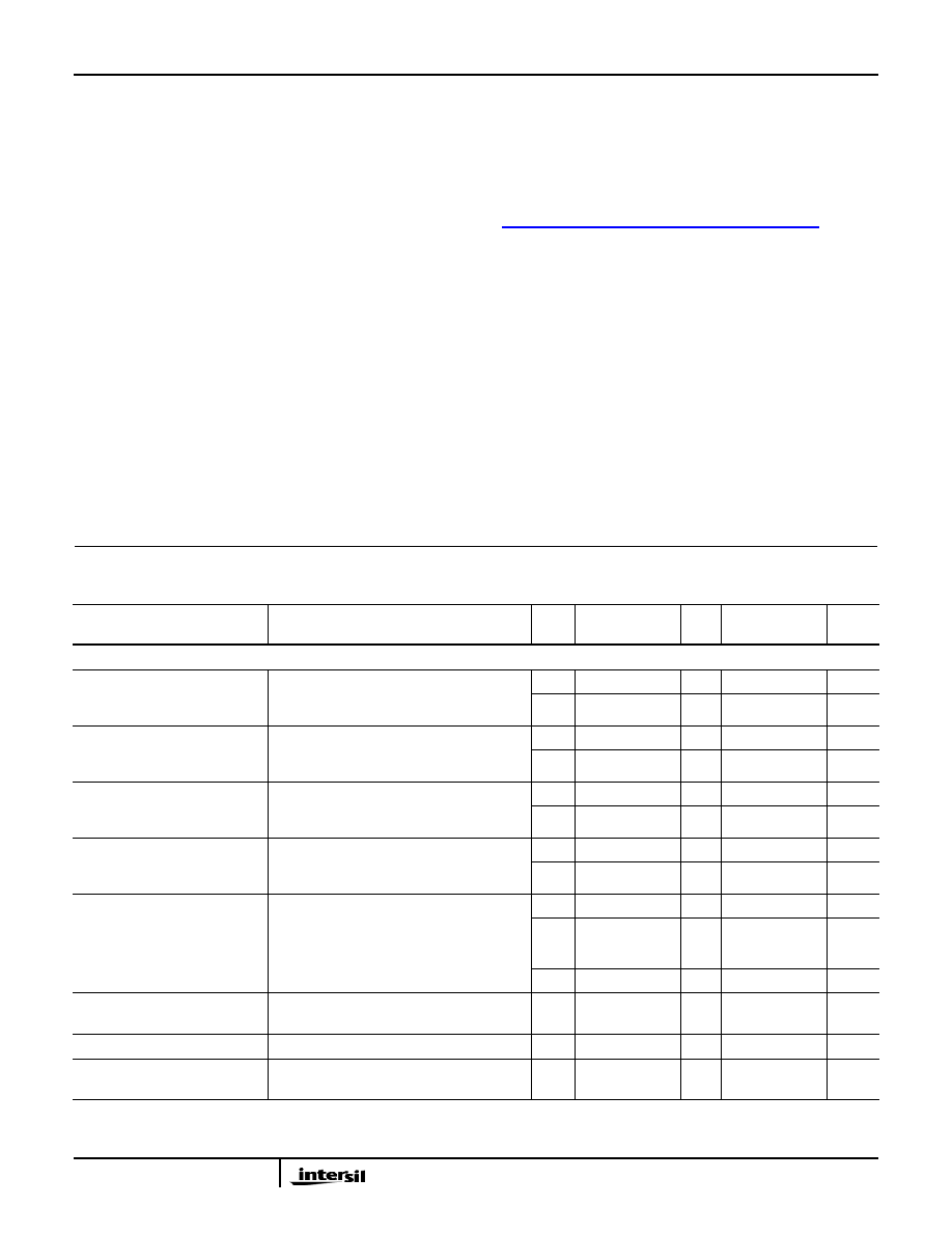
Electrical Specifications - 2.7V to 5.25V Supply Test Conditions: VDD = +3.3V, GND = 0V, VLP = GND,
VOEH =1.4V, VOEL = 0.5V, (Note 9), Unless Otherwise Specified. Boldface limits apply over the operating temperature
range, -40°C to +85°C.
PARAMETER
TEST CONDITIONS
TEMP
(°C)
MIN
(Notes 10, 11) TYP
MAX
(Notes 10, 11) UNITS
ANALOG SWITCH CHARACTERISTICS
ON-Resistance, rON
(High-Speed)
VDD = 2.7V, OE = 1.4V, IDx = 17mA,
VCom+ or VCOM- = 0V to 400mV
25
-
3.5
5
Ω
Full
-
7
Ω
rON Matching Between
Channels, ΔrON (High-Speed)
VDD = 2.7V, OE = 1.4V, IDx = 17mA,
VCom+ or VCOM- = Voltage at max rON,
(Notes 13, 14)
25
-
0.2
0.45
Ω
Full
-
0.55
Ω
rON Flatness, RFLAT(ON)
(High-Speed)
VDD = 2.7V, OE = 1.4V, IDx = 17mA,
VCom+ or VCOM- = 0V to 400mV
(Notes 12, 14)
25
-
0.26
1
Ω
Full
-
1.2
Ω
ON-Resistance, rON
VDD = 3.3V, OE = 1.4V, ICOMx = 17mA,
VCom+ or VCOM- = 3.3V
+25
-
6.8
17
Ω
Full
-
22
Ω
OFF Leakage Current, IDx(OFF) VDD = 5.25V, OE = 0V, VDx =0.3V, 3.3V,
VCOMX = 3.3V, 0.3V
25
-20
1
20
nA
Full
-
30
-
nA
ON Leakage Current, IDx(ON) VDD = 5.25V, OE = 5.25V, VDx = 0.3V,
3.3V, VCOMX = 0.3V, 3.3V
25
-9
-
9
A
Full
-12
-
12
A
Power OFF Leakage Current,
ICOM+, ICOM-
VDD = 0V, VCOM+ = 5.25V, VCOM- = 5.25V,
OE = 0V
25
-
11
A
Power OFF Logic Current, IOE VDD = 0V, OE = 5.25V
25
-
22
A
Power OFF D+/D- Current,
ID+, ID-
VDD = 0V, OE = VDD, VD+ = VD- = 5.25V 25
-
1
A
ISL54228
相关PDF资料 |
PDF描述 |
|---|---|
| VE-2WY-IV-F3 | CONVERTER MOD DC/DC 3.3V 99W |
| VE-2WY-IV-F2 | CONVERTER MOD DC/DC 3.3V 99W |
| ISL84051IBZ-T7A | IC MULTIPLEXER 8X1 16SOIC |
| ISL54233IRUZ-T7A | IC INTERFACE |
| DSPIC30F4011T-20E/ML | IC DSPIC MCU/DSP 48K 44QFN |
相关代理商/技术参数 |
参数描述 |
|---|---|
| ISL54230 | 制造商:INTERSIL 制造商全称:Intersil Corporation 功能描述:Octal Multiprotocol Switch |
| ISL54230_09 | 制造商:INTERSIL 制造商全称:Intersil Corporation 功能描述:Octal Multiprotocol Switch |
| ISL54230EVAL3Z | 功能描述:EVALUATION BOARD ISL54230 RoHS:是 类别:编程器,开发系统 >> 评估演示板和套件 系列:- 标准包装:1 系列:PCI Express® (PCIe) 主要目的:接口,收发器,PCI Express 嵌入式:- 已用 IC / 零件:DS80PCI800 主要属性:- 次要属性:- 已供物品:板 |
| ISL54230IIZ-T | 功能描述:IC USB SWITCH DPDT OCTAL 36WLCSP RoHS:是 类别:集成电路 (IC) >> 接口 - 模拟开关,多路复用器,多路分解器 系列:- 产品培训模块:Lead (SnPb) Finish for COTS Obsolescence Mitigation Program 标准包装:36 系列:- 功能:多路复用器 电路:2 x 4:1 导通状态电阻:75 欧姆 电压电源:单/双电源 电压 - 电源,单路/双路(±):2 V ~ 12 V,±2 V ~ 6 V 电流 - 电源:- 工作温度:0°C ~ 70°C 安装类型:表面贴装 封装/外壳:20-SOIC(0.295",7.50mm 宽) 供应商设备封装:20-SOIC W 包装:管件 |
| ISL54230IRTZ | 功能描述:IC SWITCH QUAD DPDT 32TQFN RoHS:是 类别:集成电路 (IC) >> 接口 - 模拟开关,多路复用器,多路分解器 系列:- 产品培训模块:Lead (SnPb) Finish for COTS Obsolescence Mitigation Program 标准包装:36 系列:- 功能:多路复用器 电路:2 x 4:1 导通状态电阻:75 欧姆 电压电源:单/双电源 电压 - 电源,单路/双路(±):2 V ~ 12 V,±2 V ~ 6 V 电流 - 电源:- 工作温度:0°C ~ 70°C 安装类型:表面贴装 封装/外壳:20-SOIC(0.295",7.50mm 宽) 供应商设备封装:20-SOIC W 包装:管件 |
发布紧急采购,3分钟左右您将得到回复。