- 您现在的位置:买卖IC网 > PDF目录11170 > ISL54302IRZ-T (Intersil)IC SWITCH QUAD SPST 20QFN PDF资料下载
参数资料
| 型号: | ISL54302IRZ-T |
| 厂商: | Intersil |
| 文件页数: | 14/16页 |
| 文件大小: | 0K |
| 描述: | IC SWITCH QUAD SPST 20QFN |
| 标准包装: | 6,000 |
| 功能: | 开关 |
| 电路: | 4 x SPST - NO |
| 导通状态电阻: | 2 欧姆 |
| 工作温度: | -40°C ~ 85°C |
| 安装类型: | 表面贴装 |
| 封装/外壳: | 20-VFQFN 裸露焊盘 |
| 供应商设备封装: | 20-QFN(4x4) |
| 包装: | 带卷 (TR) |
7
March 19, 2008
ISL54302 Detailed Description
The ISL54302 quad analog switches offer switching capability
from a split-supply -3V and +9V or single 0V and 5V to 12V
supply. Please review “Power Supply Considerations” on
page 7 before powering up the device.
The user can employ multi-device control data in two ways.
The S1-S4-CTRL lines can be connected to several devices,
with each device having its own CS-LATCH connection to
the system controller. The other way is to have separate
S1-4-CTRL connections for each switch and a single
CS-LATCH connection to all ISL54302s.
Power Supply Considerations
The ISL54302 construction consists of CMOS analog
switches and four supply pins: VPLUS, VSS, VLOGIC, VDD
and GND. VPLUS and VSS determine the switch voltage
range of the four SPST CMOS switches and set their analog
voltage limits. There are no connections between the switch
contact signal path and GND.
VLOGIC and GND power the digital input/output logic level
shifters (thus setting the digital switching point). The level
shifters convert the external logic levels to VDD and VSS
signals to drive the internal digital circuitry.
VDD and VSS power the internal logic of the device. VDD
must always be held at a fixed 3V above VSS to avoid
device damage.
Whether operating split or single device, GND will
always be @ 0V and VLOGIC will always be @ 3V.
VDD should always remain 3V above VSS. VSS to
VPLUS should not exceed a maximum spread of more
than 12V. For examples, see the following:
SPLIT POSITIVE AND NEGATIVE SWITCH RANGE
OPERATION
VSS = -3V, VDD = +0V, VPLUS = +9V, VLOGIC = 3V
VSS = -1V, VDD = +2V, VPLUS = +11V, VLOGIC = 3V
POSITIVE SWITCH RANGE OPERATION
VSS = 0V, VDD = +3V, VPLUS = +12V, VLOGIC = 3V
ISL54302 Parallel Communications
The ISL54302 operates based on parallel data. CTRL and
LATCH inputs are 3V level compatible. Setup and Hold times
relative to the rising the edge of the CS-LATCH input must
be maintained for proper operation. Switch control data is
clocked into internal registers on the rising edge of
CS-LATCH.
MULTIPLE DEVICE CONNECTION
The user can configure the four SX-CTRL inputs to connect
to several ISL54302’s. In this configuration each ISL54302
requires a separate/dedicated CS-LATCH input. Therefore,
each device will update at different times.
So in essence, the S1-S4-CTRL signals are multiplexed and
connected to all switch control inputs in parallel (see Figure 8).
For non-multiplexed connections, each SX-CTRL input must
have a dedicated logic input for each switch/each device. If
three ISL54302s are being used, the user must supply 12
dedicated SX-CTRL signals. All switches are then tied to the
same CS-LATCH pin and all devices would change state at
the same time.
ISL54302 CS-LATCH Pin Discussion
The ISL54302’s operational state does not change while
SX-CTRL inputs are changing. The user must insure that the
CS-LATCH pin remains low and does not change state while
SX-CTRL inputs are changing.
Once the user has set the SX-CTRL inputs, the CS-LATCH
pin is then utilized. Just as the CS-LATCH pin must remain
low during SX-CTRL setup, the SX-CTRL pins must remain
stable during and after the CS-LATCH operation.
The switch from present to next operation occurs on the
rising edge on the CS-LATCH pin. This rising edge transfers
data to the internal 4-bit switch control registers. This
transfer updates opening/closing of the four switches.
ISL54302 Power On Reset (POR)
Switch conditions are controlled during POR (Power On
Reset). During and after a POR condition, the switches are
opened until closed by the controller.
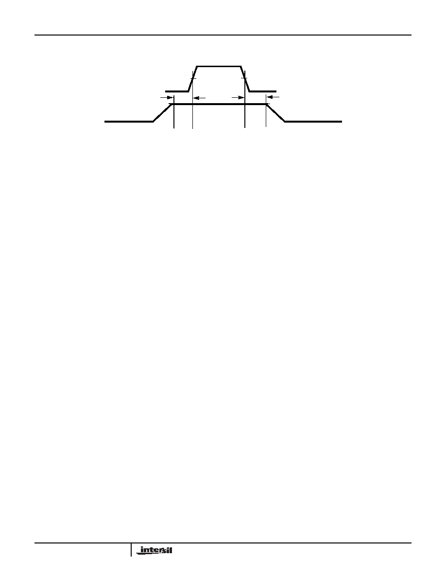
FIGURE 5. SETUP AND HOLD TIMES
Test Circuits and Waveforms (Continued)
CS-LATCH
INPUT
tSETUP
SX-CTRL
DATA = 1
100%
DATA = 0
SX-CTRL SHOULD REMAIN IN DESIRED STATE, BEFORE DURING AND AFTER CS-LATCH.
tHOLD
50%
ISL54302
相关PDF资料 |
PDF描述 |
|---|---|
| VI-JWD-IW | CONVERTER MOD DC/DC 85V 100W |
| ISL8393IBZ | IC SWITCH QUAD SPST 16SOIC |
| ISL8391IBZ | IC SWITCH QUAD SPST 16SOIC |
| PI2LVD412ZHEX | IC MUX/DEMUX QUAD 2X1 42TQFN |
| ISL43681IRZ | IC MUX/DEMUX 8X1 20QFN |
相关代理商/技术参数 |
参数描述 |
|---|---|
| ISL54400 | 制造商:INTERSIL 制造商全称:Intersil Corporation 功能描述:Low Voltage, Dual SPDT, USB/Audio Switches with Negative Signal Capability |
| ISL54400EVAL1Z | 功能描述:EVALUATION KIT FOR ISL54400 RoHS:是 类别:编程器,开发系统 >> 评估演示板和套件 系列:- 标准包装:1 系列:PCI Express® (PCIe) 主要目的:接口,收发器,PCI Express 嵌入式:- 已用 IC / 零件:DS80PCI800 主要属性:- 次要属性:- 已供物品:板 |
| ISL54400IRUZ-T | 功能描述:IC USB SWITCH DUAL SPDT 10UTQFN RoHS:是 类别:集成电路 (IC) >> 接口 - 模拟开关,多路复用器,多路分解器 系列:- 标准包装:2,500 系列:- 功能:视频交叉点开关 电路:1 x 8:6 导通状态电阻:- 电压电源:单电源 电压 - 电源,单路/双路(±):3.135 V ~ 5.25 V 电流 - 电源:55mA 工作温度:-40°C ~ 85°C 安装类型:表面贴装 封装/外壳:24-TSSOP(0.173",4.40mm 宽) 供应商设备封装:24-TSSOP 包装:带卷 (TR) 产品目录页面:1214 (CN2011-ZH PDF) 其它名称:FMS6502MTC24XTR |
| ISL54400IRZ | 功能描述:IC USB SWITCH DUAL SPDT 10TDFN RoHS:是 类别:集成电路 (IC) >> 接口 - 模拟开关,多路复用器,多路分解器 系列:- 产品培训模块:Lead (SnPb) Finish for COTS Obsolescence Mitigation Program 标准包装:36 系列:- 功能:多路复用器 电路:2 x 4:1 导通状态电阻:75 欧姆 电压电源:单/双电源 电压 - 电源,单路/双路(±):2 V ~ 12 V,±2 V ~ 6 V 电流 - 电源:- 工作温度:0°C ~ 70°C 安装类型:表面贴装 封装/外壳:20-SOIC(0.295",7.50mm 宽) 供应商设备封装:20-SOIC W 包装:管件 |
| ISL54400IRZ-T | 功能描述:IC USB SWITCH DUAL SPDT 10TDFN RoHS:是 类别:集成电路 (IC) >> 接口 - 模拟开关,多路复用器,多路分解器 系列:- 产品培训模块:Lead (SnPb) Finish for COTS Obsolescence Mitigation Program 标准包装:36 系列:- 功能:多路复用器 电路:2 x 4:1 导通状态电阻:75 欧姆 电压电源:单/双电源 电压 - 电源,单路/双路(±):2 V ~ 12 V,±2 V ~ 6 V 电流 - 电源:- 工作温度:0°C ~ 70°C 安装类型:表面贴装 封装/外壳:20-SOIC(0.295",7.50mm 宽) 供应商设备封装:20-SOIC W 包装:管件 |
发布紧急采购,3分钟左右您将得到回复。