- 您现在的位置:买卖IC网 > PDF目录383135 > ISL5585FCR (INTERSIL CORP) 3.3V Ringing SLIC Family for Voice Over Broadband VOB PDF资料下载
参数资料
| 型号: | ISL5585FCR |
| 厂商: | INTERSIL CORP |
| 元件分类: | 模拟传输电路 |
| 英文描述: | 3.3V Ringing SLIC Family for Voice Over Broadband VOB |
| 中文描述: | TELECOM-SLIC, PQCC32 |
| 封装: | 7 X 7 MM, PLASTIC, MO-220VKKC, QFN-32 |
| 文件页数: | 17/22页 |
| 文件大小: | 425K |
| 代理商: | ISL5585FCR |
17
Ringing Input
The ringing input, V
RS
, is a high impedance input. The high
impedance allows the use of low value capacitors for AC
coupling the ring signal. The V
RS
input is enabled only
during the ringing mode, therefore a free running oscillator
may be connected to VRS at all times.
When operating from a battery of -100V, each amplifier, Tip
and Ring, will swing a maximum of 95V
P-P
. Hence, the
maximum signal swing at VRS to achieve full scale ringing is
approximately 2.4V
P-P
. The low signal levels are compatible
with the output voltage range of the CODEC. The digital
nature of the CODEC ideally suits it for the function of
programmable ringing generator.
Logic Control
Ringing patterns consist of silent intervals. The ringing to
silent pattern is called the ringing cadence. During the silent
portion of ringing, the device can be programmed to any
other operating mode. The most likely candidates are low
power standby or forward active. Depending on system
requirements, the low or high battery may be selected.
Loop supervision is provided with the ring trip detector. The ring
trip detector senses the change in loop current when the phone
is taken off hook. The loop detector full wave rectifies the
ringing current, which is then filtered with external components
R
RT
and C
RT
. The resistor R
RT
sets the trip threshold and the
capacitor C
RT
sets the trip response time. Most applications will
require a trip response time less than 150ms.
Three very distinct actions occur when the devices detects a
ring trip. First, the DET output is latched low. The latching
mechanism eliminates the need for software filtering of the
detector output. The latch is cleared when the operating
mode is changed externally. Second, the VRS input is
disabled, removing the ring signal from the line. Third, the
device is internally forced to the forward active mode.
Power Dissipation
The power dissipation during ringing is dictated by the load
driving requirements and the ringing waveform. The key to valid
power calculations is the correct definition of average and RMS
currents. The average current defines the high battery supply
current. The RMS current defines the load current.
The cadence provides a time averaging reduction in the
peak power. The total power dissipation consists of ringing
power, P
r
, and the silent interval power, P
s
.
t
r
The terms t
R
and t
S
represent the cadence. The ringing
interval is t
R
and the silent interval is t
S
. The typical cadence
ratio t
R
:t
S
is 1:2.
The quiescent power of the device in the ringing mode is
defined in Equation 58.
The total power during the ringing interval is the sum of the
quiescent power and loading power:
For sinusoidal waveforms, the average current, I
AVG
, is
defined in Equation 60.
The silent interval power dissipation will be determined by
the quiescent power of the selected operating mode.
Unbalanced Ringing
The ISL5585GCM offers Unbalanced Ringing mode (010).
This feature accommodates some Analog PBX Trunk Lines
that require the Tip terminal to be held near ground for the
duration of the ringing bursts. The Tip terminal is offset to
0V’s with an internal current source that is applied to the
inverting input of the Tip amplifier. This reduces the
differential ringing gain to 40V/V. The Ring terminal will
center at Vbh/2 and swing from -Vbh to ground. As in
Balanced Ringing, off hook detection is accomplished by
sensing the peak current and comparing it to a preset
threshold. This allows the same sensing, comparing and
threshold circuitry to be used in both Ringing modes. This
mode of operation does not require any additional external
components.
Forward Loop Back
Overview
The Forward Loop Back mode (FLB, 101) provides test
capability for the device. An internal signal path is enabled
allowing for both DC and AC verification. The internal 600
terminating resistor has a tolerance of
±
20%. The device is
intended to operate from only the low battery during this
mode.
Architecture
When the forward loop back mode is initiated internal
switches connect a 600
load across the outputs of the Tip
and Ring amplifiers.
P
RNG
P
r
t
s
----+
×
P
s
t
s
r
t
s
-----+
×
+
=
(EQ. 57)
P
r Q
)
V
BH
I
BHQ
×
V
BL
I
BLQ
×
V
CC
I
CCQ
×
+
+
=
(EQ. 58)
P
r
P
r Q
)
V
BH
I
AVG
×
V
2
REN
R
LOOP
-----------------+
–
+
=
(EQ. 59)
I
AVG
π
V
Z
REN
2
×
LOOP
----------------+
=
(EQ. 60)
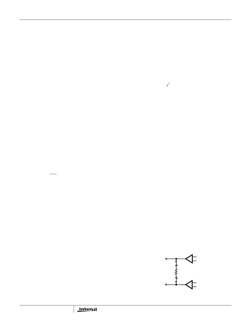
FIGURE 13. FORWARD LOOP BACK INTERNAL TERMINATION
RING AMP
TIP AMP
RING
TIP
600
ISL5585
相关PDF资料 |
PDF描述 |
|---|---|
| ISL5586BIM | Low Power Ringing SLIC for Home Gateways |
| ISL5586FCM | Low Power Ringing SLIC for Home Gateways |
| ISL5586CIM | Low Power Ringing SLIC for Home Gateways |
| ISL5586DIM | Low Power Ringing SLIC for Home Gateways |
| ISL56292IN | Dual 8-bit, +3.3V, 130/210MSPS, CommLink TM High Speed D/A Converter |
相关代理商/技术参数 |
参数描述 |
|---|---|
| ISL5585FCR-TK | 功能描述:IC SLIC RINGING 3.3V VOB 32-QFN RoHS:否 类别:集成电路 (IC) >> 接口 - 电信 系列:- 产品培训模块:Lead (SnPb) Finish for COTS 产品变化通告:Product Discontinuation 06/Feb/2012 标准包装:750 系列:* |
| ISL5585FCRZ | 制造商:Intersil Corporation 功能描述: 制造商:Intersil Corporation 功能描述:Telecom Line Management ICs RINGING SLIC W/3 3V VCC 75V/53DB |
| ISL5585FCRZ-T | 制造商:Intersil Corporation 功能描述:PB-FREE RINGING SLIC W/3.3V VCC, 75V/53DB T&R - Tape and Reel |
| ISL5585FCRZ-TK | 功能描述:IC SLIC RINGING 3.3V VOB 32-QFN RoHS:是 类别:集成电路 (IC) >> 接口 - 电信 系列:- 产品培训模块:Lead (SnPb) Finish for COTS 产品变化通告:Product Discontinuation 06/Feb/2012 标准包装:750 系列:* |
| ISL5585GCM | 制造商:Rochester Electronics LLC 功能描述: 制造商:Intersil Corporation 功能描述: |
发布紧急采购,3分钟左右您将得到回复。