- 您现在的位置:买卖IC网 > PDF目录383135 > ISL5586DIM (INTERSIL CORP) Low Power Ringing SLIC for Home Gateways PDF资料下载
参数资料
| 型号: | ISL5586DIM |
| 厂商: | INTERSIL CORP |
| 元件分类: | 模拟传输电路 |
| 英文描述: | Low Power Ringing SLIC for Home Gateways |
| 中文描述: | TELECOM-SLIC, PQCC28 |
| 封装: | PLASTIC, MS-018AB, LCC-28 |
| 文件页数: | 13/20页 |
| 文件大小: | 497K |
| 代理商: | ISL5586DIM |
4-13
Power Denial
Overview
The power denial mode (111) will shutdown the entire device
except for the logic interface. Loop supervision is not
provided. This mode may be used as a sleep mode or to
shut down the SLIC in the presence of fault conditions.
Switching between high and low battery will have no effect
during power denial.
Functionality
During power denial, both the Tip and Ring amplifiers are
disabled, presenting high impedances to the line. The
voltages at both outputs are near ground.
Thermal Shutdown
In the event the safe die temperature is exceeded due to a fault
condition the device will automatically shut down. The thermal
shutdown threshold is approximately 170
o
C.When the device
cools to a temperature below the thermal threshold it will power
back up automatically. If the fault persists the part will continue
to go in and out of thermal shutdown which can be observed as
an oscillation on Tip or Ring. Programming power denial will
shut down the device and stop the self cooling cycle.
Battery Switching
Overview
The integrated battery switch selects between high battery
and low battery operation. The battery switch is controlled with
the logic input BSEL. When BSEL is a logic high, the high
battery (V
BH
) is selected. A logic low will enable the low
battery (V
BL
). All operating modes of the SLIC will function
from high or low battery, but it is strongly recommended
Forward Loop Back be enabled only with the low battery.
Functionality
The logic control is independent of the operating mode
decode. Independent logic control provides the most
flexibility and will support all application configurations.
When changing device operating states, battery switching
should occur simultaneously with or prior to changing the
operating mode. In most cases, this will minimize overall
power dissipation and prevent glitches on the DET output.
The only external component required to support the battery
switch is a diode in series with the V
BH
supply lead. In the
event that high battery is removed, the diode allows the
device to transition to low battery operation.
Low Battery Operation
All off hook operating conditions should use the low battery
to minimize power dissipation. A typical low battery
operating voltage for the SLIC is -24V, however this may be
increased to support longer loop lengths or high loop
current requirements. Standby conditions may also operate
from the low battery if MTU compliance is not required,
further reducing standby power dissipation.
High Battery Operation
Other than ringing, the high battery should be used for
standby conditions which must provide MTU compliance.
During standby operation the power consumption is typically
85mW with -100V battery. If ringing requirements do not
require full 100V operation, then a lower battery will result in
lower standby power.
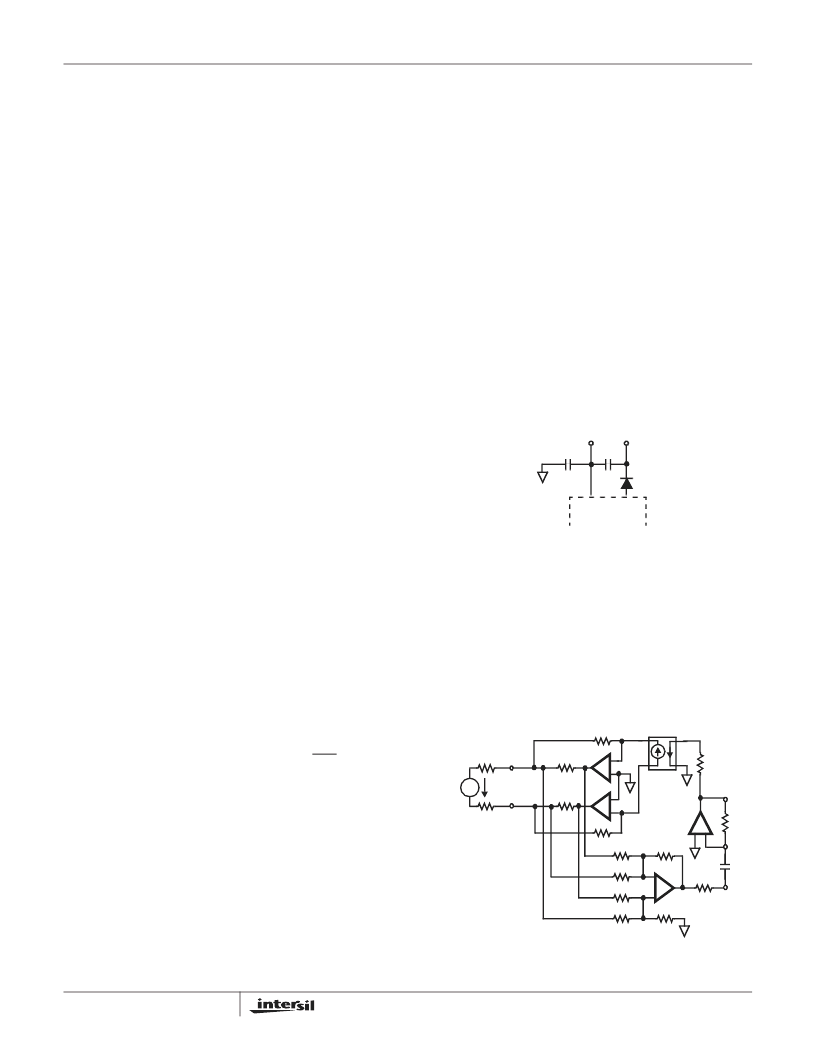
High Voltage Decoupling
The 100V rating of the SLIC dictates a capacitor of higher
voltage rating be used for decoupling. Suggested decoupling
values for all device pins are 0.1
μ
F. If the protection scheme
shown in Figure 15 is implemented the V
BH
decoupling
capacitor should be increased to 0.47uF. This is done to
minimize the turn-on time of the battrax device during
negative surge transients. Standard surface mount ceramic
capacitors are rated at 100V. For applications driven by low
cost and small size, the decoupling scheme shown in Figure
10 could be implemented.
It is important to place an external diode between the V
BH
pin
and the decoupling capacitor. Connecting the decoupling
capacitor directly to the V
BH
pin will degrade the reliability of the
device. Refer to Figure 15 for the proper arrangement. This
applies to both single and stacked and decoupling schemes.
If V
BL
and V
BH
are tied together the battery switch function
is overridden. In this case the external diode is not needed
and the decoupling capacitor may be attached directly to
V
BH
pin.
V
BH
V
BL
0.22
μ
0.22
μ
ISL5586
FIGURE 10. ALTERNATE DECOUPLING SCHEME
FIGURE 11. IMPEDANCE SYNTHESIS
TIP
RING
+
-
-IN
V
FB
V
ZO
R
F
R
R
+
-
+
-
+
-
1:1
20
20
3R
4R
4R
4R
4R
3R
8K
R
S
C
FB
T
A
V
SA
IL
V
TR
+
-
V
2W
ISL5586
相关PDF资料 |
PDF描述 |
|---|---|
| ISL56292IN | Dual 8-bit, +3.3V, 130/210MSPS, CommLink TM High Speed D/A Converter |
| ISL5629IN | Dual 8-bit, +3.3V, 130/210MSPS, CommLink TM High Speed D/A Converter |
| ISL5629EVAL1 | Dual 8-bit, +3.3V, 130/210MSPS, CommLink TM High Speed D/A Converter |
| ISL5629 | Dual 8-bit, +3.3V, 130/210+MSPS, High Speed D/A Converter(双路8位, +3.3V, 130/210+MSPS, 高速D/A转换器) |
| ISL56402IN | 3V Dual 8-Bit, 20/40/60MSPS A/D Converter with Internal Voltage Reference |
相关代理商/技术参数 |
参数描述 |
|---|---|
| ISL5586DIMZ | 功能描述:IC SLIC RINGING LP HOME 28-PLCC RoHS:是 类别:集成电路 (IC) >> 接口 - 电信 系列:RSLIC18 产品培训模块:Lead (SnPb) Finish for COTS 产品变化通告:Product Discontinuation 06/Feb/2012 标准包装:750 系列:* |
| ISL5586EVAL1 | 制造商:Intersil Corporation 功能描述:DEV TOOL, EVAL BD FOR LOW PWR RINGING SLIC FOR HOME GATEWAYS - Bulk |
| ISL5586FCM | 制造商:Rochester Electronics LLC 功能描述:RINGING SLIC FOR RESIDENTIAL HOME GATEWAYS 75V/53DB - Bulk 制造商:Intersil Corporation 功能描述: |
| ISL5586FCMT | 制造商:INTERSIL 功能描述:New |
| ISL5586FCMZ | 制造商:Intersil 功能描述:RINGING SLIC FORSIDE HOME GATEWAYS 75V |
发布紧急采购,3分钟左右您将得到回复。