参数资料
| 型号: | ISL5729/2INZ |
| 厂商: | Intersil |
| 文件页数: | 8/10页 |
| 文件大小: | 0K |
| 描述: | IC DAC 10BIT CMOS DUAL 48LQFP |
| 标准包装: | 250 |
| 位数: | 10 |
| 数据接口: | 并联 |
| 转换器数目: | 2 |
| 电压电源: | 模拟和数字 |
| 功率耗散(最大): | 274mW |
| 工作温度: | -40°C ~ 85°C |
| 安装类型: | 表面贴装 |
| 封装/外壳: | 48-LQFP |
| 供应商设备封装: | 48-TQFP(7x7) |
| 包装: | 托盘 |
| 输出数目和类型: | * |
| 采样率(每秒): | 210M |
2011 Fairchild Semiconductor Corporation
www.fairchildsemi.com
FT3001 Rev. 1.0.4
7
FT3001
—
Reset
Timer
with
Configurable
Delay
Functional Description
The reset timer uses an internal oscillator and a two-
stage 21-bit counter to determine when the output pins
switch. The time, n, is set by the hard-wired logic level
of the DSR0 and DSR1 pins. See Table 1 & 2.
Table 1.
FT3001UMX Truth Table
DSR0
DSR1
Reset Time (
20%)
in Seconds
0
3.00
0
1
3.75
1
0
4.50
1
6.00
Table 2.
FT3001MPX Truth Table
DSR0
Reset Time (
20%)
in Seconds
0
3.0
1
4.5
The two CMOS input pins, /SR0 and /SR1, control the
reset function. A low input signal on both /SR0 and /SR1
starts the oscillator. Both /SR0 and /SR1 pins must be
held LOW for time n before the /RST1 and RST2
outputs are activated. The TRIG pin should be tied LOW
during normal operation. The TRIG pin is used for
SCAN testing.
Application Information
IMPORTANT
: The DSR0 and DSR1 pins must be tied
directly to VCC or GND to provide a HIGH or LOW
voltage level. The voltage level on the DSR pin
determines the length of the configurable delay. The
voltage level on the DSR pins must not change during
normal operation. Do not use pull-up or pull-down
resistors on DSR pins.
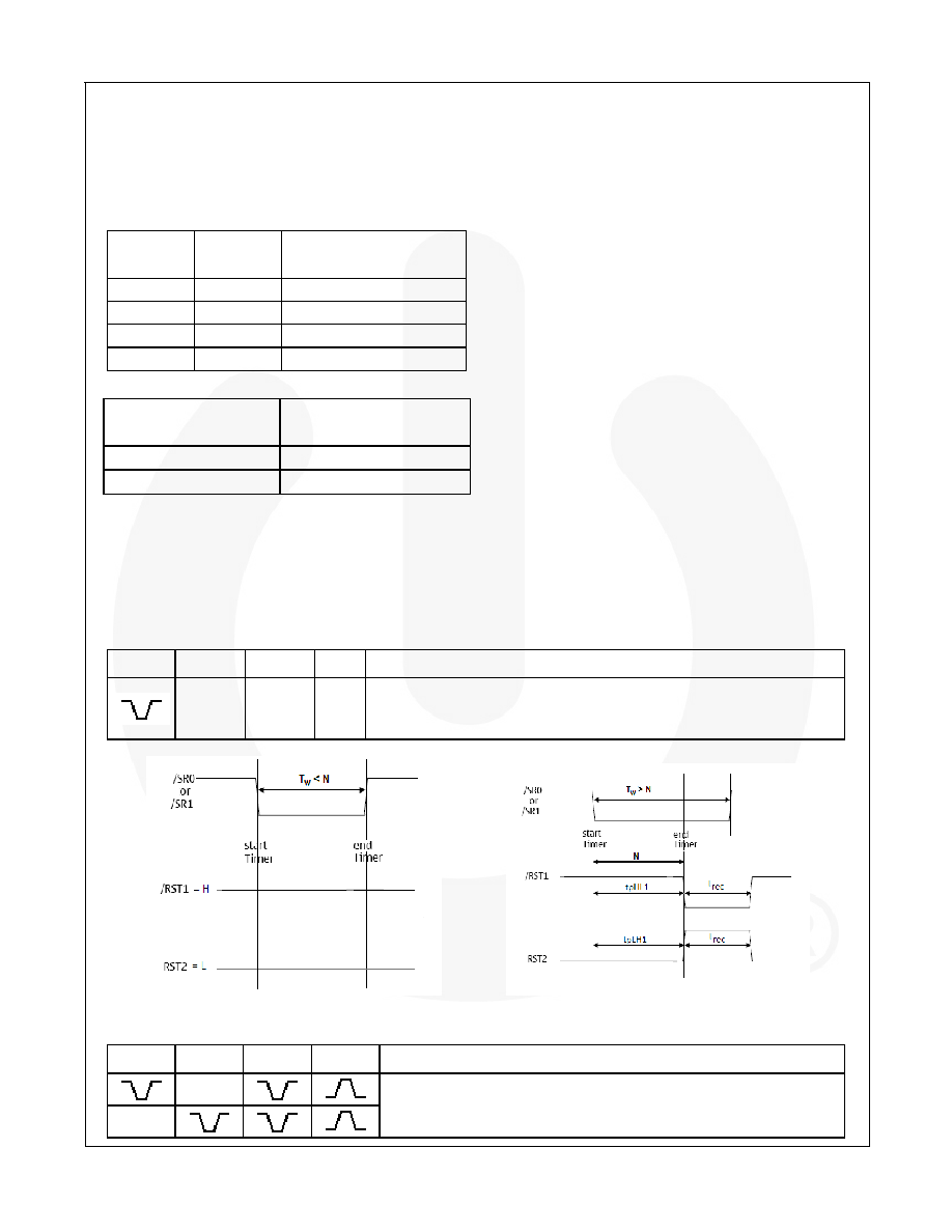
Short Duration (Button Press Time < n)
In this case, both input /SR0 and /SR1 are LOW for a
duration (tW) that is shorter than time n. When an input
goes LOW, the internal timer starts counting. If the input
goes HIGH before time n, the timer stops counting and
resets and no changes occur on the outputs.
Long Duration (tW > n)
In this case, both input /SR0 and /SR1 are LOW for a
duration (tW) that is longer than time n. When an input
goes LOW, the internal timer starts counting.
After time n, the outputs switch and the timer stops
counting. After time tREC, the outputs return to their
original states.
Table 3.
Short Duration
/SR0
/SR1
/RST1
RST2
Description
L
H
L
The timer starts counting when both inputs go LOW. The timer stops
counting and resets when either input goes high. No changes occur on the
outputs. Both /SR0 and /SR1 need to be LOW to activate (start) the timer.
Figure 8. Short Duration
Figure 9. Long Duration
Table 4.
Long Duration
/SR0
/SR1
/RST1
RST2
Description
L
The timer starts counting when both inputs go LOW. After time n, the
outputs switch. After time tREC, the outputs return to their original states.
Both /SR0 and /SR1 need to be LOW to activate (start) the timer.
L
相关PDF资料 |
PDF描述 |
|---|---|
| ISL5757IBZ | IC DAC 10BIT 260MHZ 28-SOIC |
| ISL5761/2IBZ | CONV D/A 10BIT HS LP 28-SOIC |
| ISL5827INZ | IC DAC DUAL 12BIT 3.3V 48-LQFP |
| ISL5857IAZ | IC DAC 12-BIT 260MSPS 28-TSSOP |
| ISL5861/2IBZ | IC DAC 12BIT 210MSPS 28-SOIC |
相关代理商/技术参数 |
参数描述 |
|---|---|
| ISL5729EVAL1 | 功能描述:EVALUATION PLATFORM FOR ISL5729 RoHS:否 类别:编程器,开发系统 >> 评估板 - 数模转换器 (DAC) 系列:CommLink™ 产品培训模块:Lead (SnPb) Finish for COTS Obsolescence Mitigation Program 标准包装:1 系列:- DAC 的数量:4 位数:12 采样率(每秒):- 数据接口:串行,SPI? 设置时间:3µs DAC 型:电流/电压 工作温度:-40°C ~ 85°C 已供物品:板 已用 IC / 零件:MAX5581 |
| ISL5729IN | 功能描述:IC DAC DUAL 10BIT 3.3V 48-MQFP RoHS:否 类别:集成电路 (IC) >> 数据采集 - 数模转换器 系列:- 标准包装:2,400 系列:- 设置时间:- 位数:18 数据接口:串行 转换器数目:3 电压电源:模拟和数字 功率耗散(最大):- 工作温度:-40°C ~ 85°C 安装类型:表面贴装 封装/外壳:36-TFBGA 供应商设备封装:36-TFBGA 包装:带卷 (TR) 输出数目和类型:* 采样率(每秒):* |
| ISL5729INZ | 功能描述:IC DAC 10BIT CMOS DUAL 48LQFP RoHS:是 类别:集成电路 (IC) >> 数据采集 - 数模转换器 系列:- 产品培训模块:Lead (SnPb) Finish for COTS Obsolescence Mitigation Program 标准包装:1,000 系列:- 设置时间:1µs 位数:8 数据接口:串行 转换器数目:8 电压电源:双 ± 功率耗散(最大):941mW 工作温度:0°C ~ 70°C 安装类型:表面贴装 封装/外壳:24-SOIC(0.295",7.50mm 宽) 供应商设备封装:24-SOIC W 包装:带卷 (TR) 输出数目和类型:8 电压,单极 采样率(每秒):* |
| ISL5740 | 制造商:INTERSIL 制造商全称:Intersil Corporation 功能描述:3V Dual 10-Bit, 20/40/60MSPS A/D Converter with Internal Voltage Reference |
| ISL57402IN | 制造商:INTERSIL 制造商全称:Intersil Corporation 功能描述:3V Dual 10-Bit, 20/40/60MSPS A/D Converter with Internal Voltage Reference |
发布紧急采购,3分钟左右您将得到回复。