- 您现在的位置:买卖IC网 > PDF目录17050 > ISL5829EVAL1 (Intersil)EVALUATION PLATFORM ISL5829 HS PDF资料下载
参数资料
| 型号: | ISL5829EVAL1 |
| 厂商: | Intersil |
| 文件页数: | 2/3页 |
| 文件大小: | 0K |
| 描述: | EVALUATION PLATFORM ISL5829 HS |
| 标准包装: | 1 |
| 系列: | CommLink™ |
| DAC 的数量: | 2 |
| 位数: | 12 |
| 采样率(每秒): | 210M |
| 数据接口: | 并联 |
| DAC 型: | 电流 |
| 工作温度: | -40°C ~ 85°C |
| 已供物品: | 板 |
| 已用 IC / 零件: | ISL5829 |
�� �
�
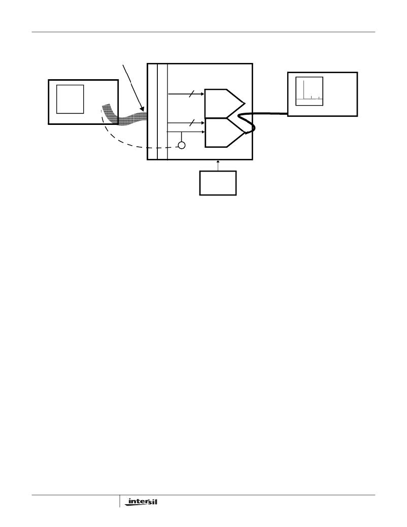
�Application� Note� AN9997�
�GORE� QUIETZONE� TM� CABLES�
�PATTERN� GENERATOR�
�ISL5x29� EVALUATION� BOARD�
�8-14� BITS�
�50� ?�
�SMA�
�CABLE�
�1/2� ISL5x29�
�DAC�
�8-14� BITS�
�SPECTRUM� ANALYZER�
�1/2� ISL5x29�
�OPTIONAL�
�DIRECT� CLK�
�CABLE�
�CLOCK�
�DAC�
�+3.3V�
�POWER�
�SUPPLY�
�FIGURE� 1.� INTERSIL� ISL5x29� EVALUATION� SYSTEM� SETUP� BLOCK� DIAGRAM�
�Board� Options�
�Jumpers� (Default� State)�
�J19� -� Selects� DAC� Sleep� Mode� (OPEN)�
�J21� -Selects� External� Reference� (OPEN)�
�J20� -� Selects� Internal� Reference� (SHORT)�
�J17,� J5� -� Selects� IOUTA,� QOUTA� (SHORT)�
�J15,� J4� -� Selects� IOUTB,� QOUTB� (SHORT)�
�J8,� J14� -� Grounds� the� Transformer� Output� (SHORT)�
�J23-J27� -� Selects� Clock� Path� and� Termination�
�Output� Transformer�
�T1,� 4� -� T1-1T� (case� style� Mini-Circuits� KK81)�
�T2,� 3� -� ADT1-1WT� (case� style� Mini-Circuits� CD542)�
�Clock� Input�
�2x20� Pin� Headers� J1� or� J3� (pin� 19)�
�SMA� -� J2�
�Clock� Output�
�SMA� -� J22�
�RSET�
�Fixed� Resistor� -� R91� (1.91k� ?� =� 20mA� full� scale� output)�
�Potentiometer� -� R90�
�Power� Supply-�
�Split� AVDD� and� DVDD�
�Single� VDD� (by� installing� R63)�
�2�
�Clock�
�The� clock� circuitry� on� the� ISL5x29eval1� is� designed� for� a�
�couple� of� options� to� be� available.� One� option� allows� a� high�
�quality� clock� signal� to� be� connected� directly� to� J2.� The�
�combination� of� jumpers� and� resistors� surrounding� J2� allows�
�the� user� to� create� a� 50� ?� power� splitter� so� the� same� clock�
�can� be� fed� off� the� board� (J22)� to� clock� the� digital� pattern�
�source� without� reflections� causing� degradations� in� DAC�
�performance.�
�To� use� the� 50� ?� power� splitter� connect� the� clock� source� to� J2.�
�Make� sure� that� R16,� R31,� and� R32� are� ~17� ?� .� Populate�
�jumpers� J24� and� J25.� Do� not� populate� J23,� J26,� or� J27.� With�
�C20,� R47,� and� R48� populated,� the� clock� will� be� biased� at� the�
�DAC� clock� input,� so� the� clock� source� does� not� have� to� be� DC�
�biased.� If� using� J2� as� the� clock� input� but� not� using� J22� to�
�clock� an� external� device,� populate� jumper� J27� so� the�
�impedance� of� the� power� splitter� is� maintained.�
�Another� option� is� to� bring� the� clock� on� the� board� via� the�
�ribbon� cables.� Choose� pin� 19� of� J1� or� J3,� but� not� both.�
�Populate� the� necessary� jumper� to� connect� pin� 19� to� the� DAC�
�clock� input� (J23� if� via� J1� or� J26� if� via� J3).� Do� not� populate�
�J24� or� J25� (unless� 50� ?� termination� is� desired).�
�Digital� Inputs�
�The� digital� inputs� are� expecting� 3V� CMOS� levels� in� offset�
�binary� format.� The� board� is� shipped� without� termination�
�resistors� so� that� most� systems� can� drive� the� load.� The� board�
�is� configured� so� the� user� can� populate� 50� ?� termination�
�resistors� if� required.� Consult� the� datasheet� for� the� DAC� for�
�min/max� amplitude� requirements� for� the� clock� and� data.�
�相关PDF资料 |
PDF描述 |
|---|---|
| ISL5729EVAL1 | EVALUATION PLATFORM FOR ISL5729 |
| REC5-0509DRW/H2/A | CONV DC/DC 5W 4.5-9VIN +/-09VOUT |
| EVB9S08DZ60 | BOARD EVAL FOR 9S08DZ60 |
| REC5-0505DRW/H2/C | CONV DC/DC 5W 4.5-9VIN +/-05VOUT |
| EVAL-AD7763EDZ | BOARD EVAL CONTROL AD7763 |
相关代理商/技术参数 |
参数描述 |
|---|---|
| ISL5829IN | 功能描述:IC DAC DUAL 12BIT 3.3V 48-MQFP RoHS:否 类别:RF/IF 和 RFID >> RF 其它 IC 和模块 系列:- 标准包装:100 系列:* |
| ISL5829INZ | 功能描述:IC CONV DUAL 12BIT 3.3V 48-LQFP RoHS:是 类别:RF/IF 和 RFID >> RF 其它 IC 和模块 系列:- 标准包装:100 系列:* |
| ISL58303DRTZ | 功能描述:IC LASER DRVR 3CHAN 24TQFN RoHS:是 类别:集成电路 (IC) >> PMIC - 激光驱动器 系列:- 产品培训模块:Lead (SnPb) Finish for COTS Obsolescence Mitigation Program 标准包装:60 系列:- 类型:激光二极管驱动器 数据速率:- 通道数:4 电源电压:3.3V 电流 - 电源:- 电流 - 调制:- 电流 - 偏置:- 工作温度:0°C ~ 70°C 封装/外壳:40-TQFN 裸露焊盘 供应商设备封装:40-TQFN EP 包装:托盘 安装类型:表面贴装 |
| ISL58303DRTZ-T13 | 功能描述:IC LASER DRVR 3CHAN 24TQFN RoHS:是 类别:集成电路 (IC) >> PMIC - 激光驱动器 系列:- 产品培训模块:Lead (SnPb) Finish for COTS Obsolescence Mitigation Program 标准包装:60 系列:- 类型:激光二极管驱动器 数据速率:- 通道数:4 电源电压:3.3V 电流 - 电源:- 电流 - 调制:- 电流 - 偏置:- 工作温度:0°C ~ 70°C 封装/外壳:40-TQFN 裸露焊盘 供应商设备封装:40-TQFN EP 包装:托盘 安装类型:表面贴装 |
| ISL58303DRTZ-T7A | 功能描述:IC LASER DRVR 3CHAN 24TQFN RoHS:是 类别:集成电路 (IC) >> PMIC - 激光驱动器 系列:- 产品培训模块:Lead (SnPb) Finish for COTS Obsolescence Mitigation Program 标准包装:60 系列:- 类型:激光二极管驱动器 数据速率:- 通道数:4 电源电压:3.3V 电流 - 电源:- 电流 - 调制:- 电流 - 偏置:- 工作温度:0°C ~ 70°C 封装/外壳:40-TQFN 裸露焊盘 供应商设备封装:40-TQFN EP 包装:托盘 安装类型:表面贴装 |
发布紧急采购,3分钟左右您将得到回复。