参数资料
| 型号: | ISL59446IRZ-T7 |
| 厂商: | Intersil |
| 文件页数: | 2/13页 |
| 文件大小: | 0K |
| 描述: | IC AMP MUX 4:1 500MHZ 32-QFN |
| 标准包装: | 1 |
| 应用: | 4:1 多路复用器-放大器 |
| 电路数: | 3 |
| -3db带宽: | 620MHz |
| 转换速率: | 1600 V/µs |
| 电流 - 电源: | 44mA |
| 电流 - 输出 / 通道: | 135mA |
| 安装类型: | 表面贴装 |
| 封装/外壳: | 32-VFQFN 裸露焊盘 |
| 供应商设备封装: | 32-QFN 裸露焊盘(5x6) |
| 包装: | 标准包装 |
| 产品目录页面: | 1235 (CN2011-ZH PDF) |
| 其它名称: | ISL59446IRZ-T7DKR |
10
FN6261.2
June 5, 2012
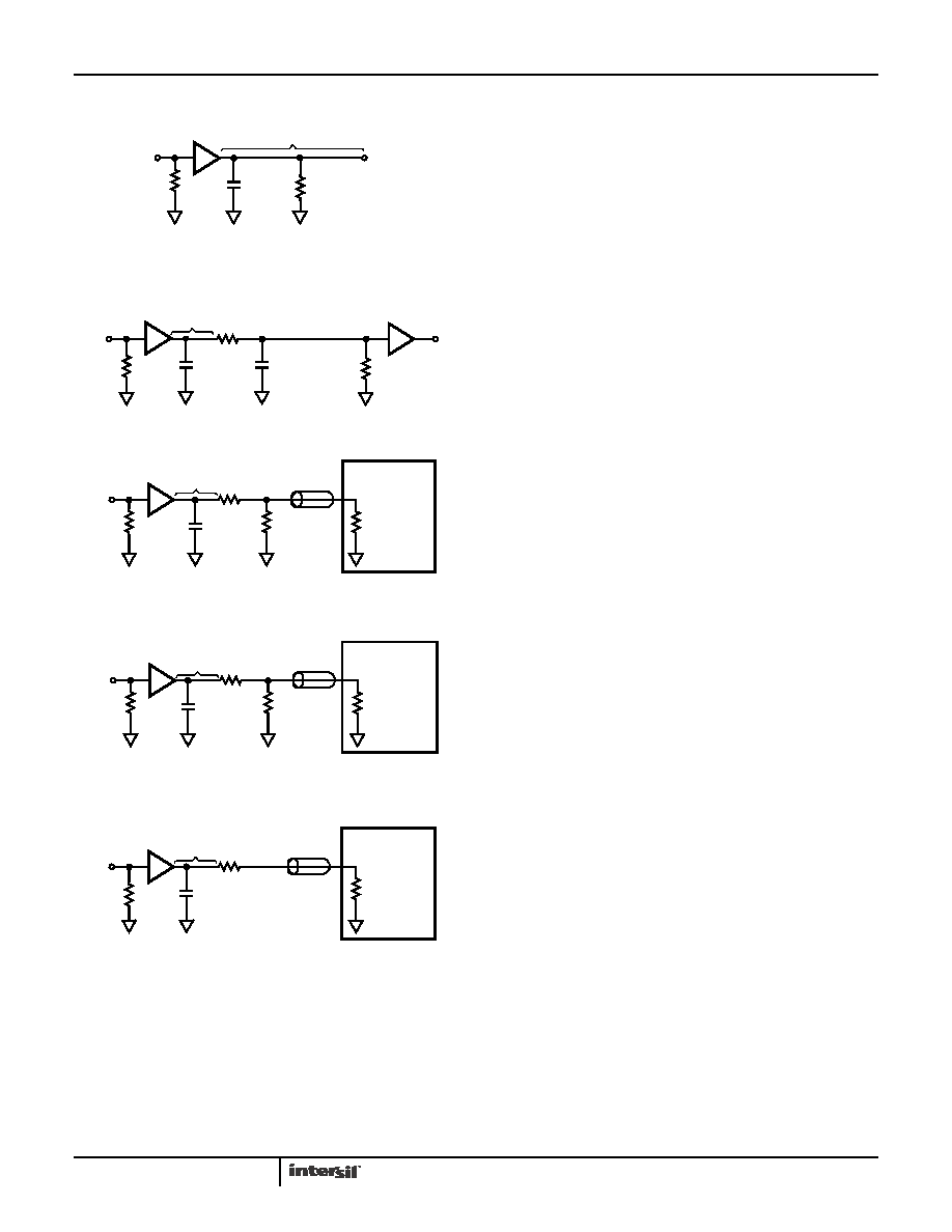
AC Test Circuits
testing AC performance at 500
Ω and 150Ω loads.
Figure 28E illustrates the optimum output load for 50
Ω and
75
Ω cable-driving.
Application Information
General
Key features of the ISL59446 include a fixed gain of 2,
buffered high impedance analog inputs and excellent AC
performance at output loads down to 150
Ω for video
cable-driving. The current feedback output amplifiers are
stable operating into capacitive loads.
For the best isolation and crosstalk rejection, all GND pins
and NIC pins must connect to the GND plane.
AC Design Considerations
High speed current-feed amplifiers are sensitive to
capacitance at the inverting input and output terminals. The
ISL59446 has an internally set gain of 2, so the inverting
input is not accessible. Capacitance at the output terminal
increases gain peaking (Figure 1) and pulse overshoot
optimized for a total output capacitance of up to 2.1pF over
the load range of 150
Ω to 500Ω. When PCB trace
capacitance and component capacitance exceed 2pF, pulse
overshoot becomes strongly dependent on the input pulse
amplitude and slew rate. This effect is shown in Figures 19
and 20, which show approximate pulse overshoot as a
function of input slew rate and output capacitance. Fast
pulse rise and fall times (<150ns) at input amplitudes above
0.2V, cause the input pulse slew rate to exceed the
1600V/s output slew rate of the ISL59446. At 125ps rise
time, pulse input amplitudes >0.2V cause slew rate limit
operation. Increasing levels of output capacitance reduce
stability resulting in increased overshoot, and settling time.
PC board trace length should be kept to a minimum in order
to minimize output capacitance and prevent the need for
controlled impedance lines. At 500MHz trace lengths
approaching 1” begin exhibiting transmission line behavior
and may cause excessive ringing if controlled impedance
traces are not used. Figure 28A shows the optimum
inter-stage circuit when the total output trace length is less
than the critical length of the highest signal frequency.
For applications where pulse response is critical and where
inter-stage distances exceed LCRIT, the circuit shown in
capacitance seen by the amplifier output to the trace
capacitance from the output pin to the resistor. Therefore,
RS should be placed as close to the ISL59446 output pin as
possible. For inter-stage distances much greater than LCRIT,
the back-loaded circuit shown in Figure 28E should be used
with controlled impedance PCB lines, with RS and RL equal
to the controlled impedance.
For applications where inter-stage distances are long, but
pulse response is not critical, capacitor CS can be added to
low values of RS to form a low-pass filter to dampen pulse
overshoot. This approach avoids the need for the large gain
correction required by the -6dB attenuation of the
AC Test Circuits
FIGURE 28A. TEST CIRCUIT WITH OPTIMAL OUTPUT LOAD
FIGURE 28B. INTER-STAGE APPLICATION CIRCUIT
FIGURE 28C. 500
Ω TEST CIRCUIT WITH 50Ω LOAD
FIGURE 28D. 150Ω TEST CIRCUIT WITH 50
Ω LOAD
FIGURE 28E. BACKLOADED TEST CIRCUIT FOR 75
Ω VIDEO
CABLE APPLICATION
ISL59446
*CL
50
Ω
VIN
500
Ω, or
RL
1.1pF
or
75
Ω
150
Ω
*CL Includes PCB trace capacitance
VOUT
LCRIT
x2
ISL59446
CS
50
Ω
VIN
500
Ω, or
RL
or
75
Ω
75
Ω
LCRIT
RS
CL
x2
ISL59446
RS
*CL
VIN
475
Ω
TEST
1.1pF
50
Ω
56.2
Ω
50
Ω
EQUIPMENT
*CL Includes PCB trace capacitance
LCRIT
x2
ISL59446
RS
*CL
VIN
118
Ω
TEST
2.1pF
50
Ω,or
86.6
Ω
50
Ω
EQUIPMENT
75
Ω
*CL Includes PCB trace capacitance
LCRIT
x2
ISL59446
RS
*CL
VIN
50
Ω or 75Ω
TEST
2.1pF
50
Ω
or
75
Ω
50
Ω or 75Ω
EQUIPMENT
*CL Includes PCB trace capacitance
LCRIT
x2
ISL59446
相关PDF资料 |
PDF描述 |
|---|---|
| EL4543IUZ | IC DVR TRPL DIFF TW-PAIR 24-QSOP |
| HA5023IBZ | IC OPAMP DUAL 125MHZ VIDEO 8SOIC |
| AD7534JPZ-REEL | IC DAC 14BIT MULT W/BUFF 20PLCC |
| ISL59837IAZ | IC VIDEO DRIVER TRUE SGL 16-QSOP |
| LTC1596-1ACN | IC D/A CONV 16BIT MLTPLYNG 16DIP |
相关代理商/技术参数 |
参数描述 |
|---|---|
| ISL59448 | 制造商:INTERSIL 制造商全称:Intersil Corporation 功能描述:500MHz Triple 2:1 Gain-of-2, Multiplexing Amplifier |
| ISL59448EVAL1Z | 功能描述:EVAL BOARD 1 FOR ISL59448 RoHS:是 类别:编程器,开发系统 >> 评估演示板和套件 系列:* 标准包装:1 系列:PCI Express® (PCIe) 主要目的:接口,收发器,PCI Express 嵌入式:- 已用 IC / 零件:DS80PCI800 主要属性:- 次要属性:- 已供物品:板 |
| ISL59448IAZ | 功能描述:IC AMP TRIPLE MUX 500MHZ 24-QSOP RoHS:是 类别:集成电路 (IC) >> 线性 - 放大器 - 视频放大器和频缓冲器 系列:- 产品培训模块:Lead (SnPb) Finish for COTS Obsolescence Mitigation Program 标准包装:50 系列:- 应用:TFT-LCD 面板:VCOM 驱动器 输出类型:满摆幅 电路数:1 -3db带宽:35MHz 转换速率:40 V/µs 电流 - 电源:3.7mA 电流 - 输出 / 通道:1.3A 电压 - 电源,单路/双路(±):9 V ~ 20 V,±4.5 V ~ 10 V 安装类型:表面贴装 封装/外壳:8-TSSOP,8-MSOP(0.118",3.00mm 宽)裸露焊盘 供应商设备封装:8-uMax-EP 包装:管件 |
| ISL59448IAZ-T7 | 功能描述:IC AMP MUX 2:1 500MHZ 24-QSOP RoHS:是 类别:集成电路 (IC) >> 线性 - 放大器 - 视频放大器和频缓冲器 系列:- 标准包装:1,000 系列:- 应用:驱动器 输出类型:差分 电路数:3 -3db带宽:350MHz 转换速率:1000 V/µs 电流 - 电源:14.5mA 电流 - 输出 / 通道:60mA 电压 - 电源,单路/双路(±):5 V ~ 12 V,±2.5 V ~ 6 V 安装类型:表面贴装 封装/外壳:20-VFQFN 裸露焊盘 供应商设备封装:20-QFN 裸露焊盘(4x4) 包装:带卷 (TR) |
| ISL59450 | 制造商:INTERSIL 制造商全称:Intersil Corporation 功能描述:Multiformat Video Crosspoint with Integrated Sync Separator |
发布紧急采购,3分钟左右您将得到回复。