- 您现在的位置:买卖IC网 > PDF目录16341 > ISL59911IRZ-EVALZ (Intersil)EVALUATION BOARD FOR ISL59911 PDF资料下载
参数资料
| 型号: | ISL59911IRZ-EVALZ |
| 厂商: | Intersil |
| 文件页数: | 13/17页 |
| 文件大小: | 0K |
| 描述: | EVALUATION BOARD FOR ISL59911 |
| 标准包装: | 1 |
ISL59911
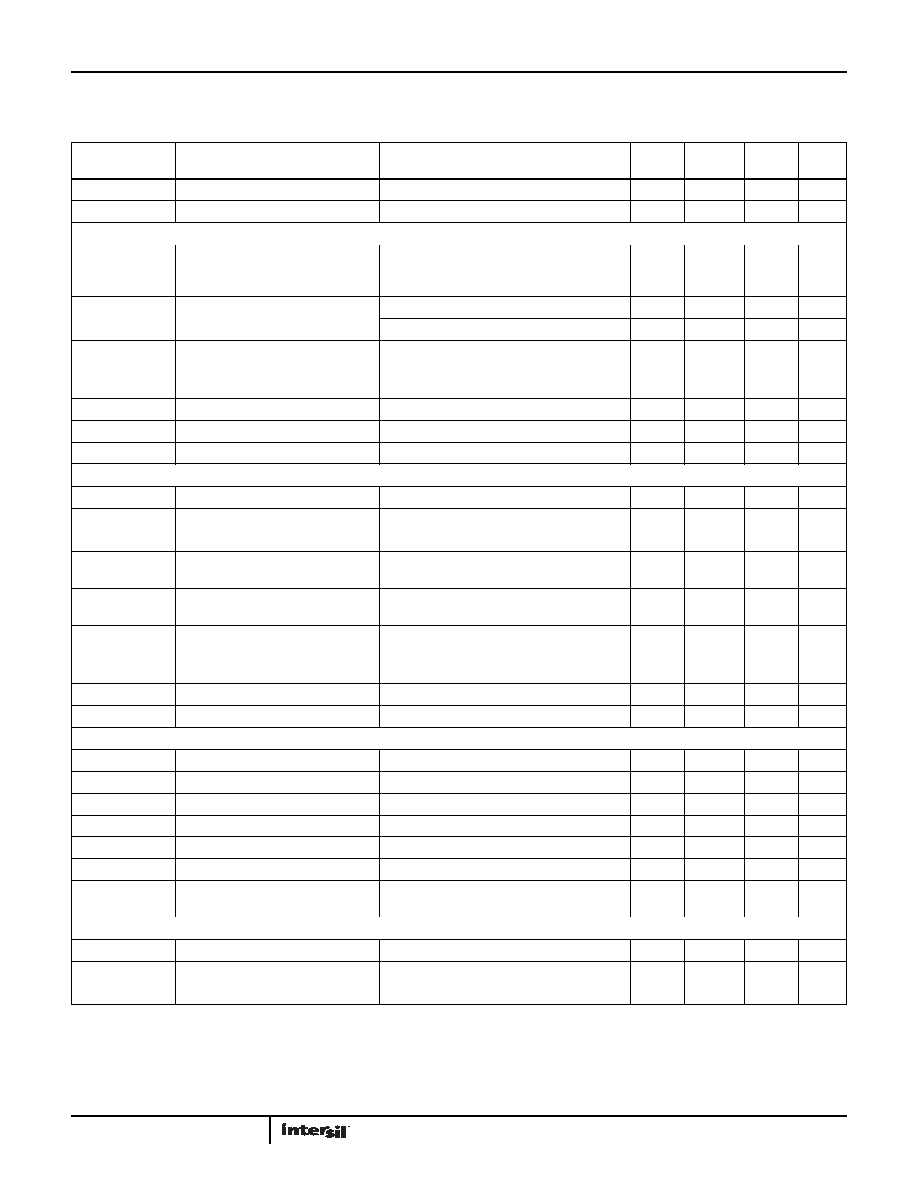
5
FN7548.0
September 2, 2011
BWCM
Common Mode Amplifier Bandwidth
10k || 5pF load
24
MHz
SRCM
Common Mode Slew Rate
VIN = -0.5V to +1.5V
0.1
V/ns
INPUT CHARACTERISTICS
CMIR
Common-mode Input Range
Differential signal passed undistorted.
Effective headroom is reduced by the p-p
amplitude of differential swing divided by 2.
-3.2/+4.0
V
CMRR
Common-mode Rejection Ratio
Measured at 100kHz
88
dB
Measured at 10MHz
58
dB
CINDIFF
Differential Input Capacitance
Capacitance between VINP and VINM
0.5
pF
RINDIFF
Differential Input Resistance
Resistance between VIN+ and VIN-
(due to common mode input resistance)
20
k
Ω
CINCM
CM Input Capacitance
Capacitance from VIN+ and VIN- to GND
1.3
pF
RINCM
CM Input Resistance
Resistance from VIN+ and VIN- to GND
25
k
Ω
VINDIFF_P-P
Max P-P Differential Input Range
Delta VIN+ - VIN- when slope gain falls to 0.9
1.9
V
OUTPUT CHARACTERISTICS
VOUT
Output Voltage Swing
±2.75
V
IOUT
Output Drive Current
RL = 10Ω, VIN+ - VIN- = ±2V
±22
mA
V(VOUT)OS
Output Offset Voltage
Post-offset calibration
-20
-8
+5
mV
R(VCM)
CM Output Resistance of VCM_R/G/B
(CM Output Mode)
At 100kHz
2.5
Ω
Gain
x1 mode
x2 mode
0.95
1.9
1.0
2.0
1.05
2.1
V/V
ΔGain
Channel-to-Channel Gain Mismatch
x1 and x2 modes
±3
%
ONOISE
Integrated Noise at Output
Inputs @ GND through 50
Ω.
0m of Equalization (Nominal)
300m of Equalization
4
20
mVRMS
SYNCOUTHI
High Level output on VS/HSOUT
10k || 5pF load, SYNC Output Mode
V+ - 1.5
V
SYNCOUTLO
Low Level output on VS/HSOUT
10k || 5pF load, SYNC Output Mode
0.4
V
SCL, SDA PINS
fMAX
Maximum I2C Operating Frequency
400
kHz
VOL
SDA Output Low Level
VSINK = 6mA
0.4
V
VIH
Input High Level
3V
VIL
Input Low Level
1.5
V
VHYST
Input Hysteresis
0.55
V
ILEAKAGE
Input Leakage Current
±1
A
tGLITCH
Maximum Width of Glitch on SCL (or
SDA) Guaranteed to be Rejected
50
ns
ENABLE, ADDR0, ADDR1 PINS
VIH
Input High Level
3V
VIL
Input Low Level
0.8
V
ILEAKAGE
Input Leakage Current
±1
A
NOTE:
7. Compliance to datasheet limits is assured by one or more methods: production test, characterization and/or design.
Electrical Specifications V+ = V+R = V+G = V+B = +5V, V- = V-R = V-G = V-B = V-D = -5V, TA = +25°C, all registers at default settings
(equalizer stages set to minimum boost, noise filter set to max bandwidth, x2 gain mode, GAINDC = 0dB), all analog inputs at 0V, auto offset
calibration executed, RL = 5pF || (75Ω + 75Ω) to GND, thermal pad connected to -5V, unless otherwise specified. (Continued)
PARAMETER
DESCRIPTION
CONDITIONS
MIN
(Note 7)
TYP
MAX
(Note 7)
UNIT
相关PDF资料 |
PDF描述 |
|---|---|
| ISL59913IRZ-EVALZ | EVAL BOARD FOR ISL59913IRZ |
| ADM6316DZ31ARJZ-R7 | IC SUPERVISOR WATCHDOG SOT23-5 |
| ISL59910IRZ-EVALZ | EVAL BOARD FOR ISL59911IRZ |
| VI-B73-EY-S | CONVERTER MOD DC/DC 24V 50W |
| ISL59833IAZ-EVALZ | EVAL BOARD FOR ISL59833IAZ |
相关代理商/技术参数 |
参数描述 |
|---|---|
| ISL59911IRZ-T7 | 功能描述:视频 IC ISL9519C EVALRD 1 50LD BATRY CHRGR RoHS:否 制造商:Fairchild Semiconductor 工作电源电压:5 V 电源电流:80 mA 最大工作温度:+ 85 C 封装 / 箱体:TSSOP-28 封装:Reel |
| ISL59913 | 制造商:INTERSIL 制造商全称:Intersil Corporation 功能描述:Triple Differential Receiver/Equalizer |
| ISL59913IRZ | 功能描述:视频 IC ISL95210 5V/10AUCK FET INDSTRL TEMP RNG RoHS:否 制造商:Fairchild Semiconductor 工作电源电压:5 V 电源电流:80 mA 最大工作温度:+ 85 C 封装 / 箱体:TSSOP-28 封装:Reel |
| ISL59913IRZ-EVALZ | 功能描述:EVAL BOARD FOR ISL59913IRZ RoHS:是 类别:编程器,开发系统 >> 评估演示板和套件 系列:* 标准包装:1 系列:PCI Express® (PCIe) 主要目的:接口,收发器,PCI Express 嵌入式:- 已用 IC / 零件:DS80PCI800 主要属性:- 次要属性:- 已供物品:板 |
| ISL59913IRZ-T7 | 功能描述:视频 IC ISL95210 5V/10AUCK FET INDSTRL TEMP RNG RoHS:否 制造商:Fairchild Semiconductor 工作电源电压:5 V 电源电流:80 mA 最大工作温度:+ 85 C 封装 / 箱体:TSSOP-28 封装:Reel |
发布紧急采购,3分钟左右您将得到回复。