- 您现在的位置:买卖IC网 > PDF目录176103 > ISL6144 (Intersil Corporation) High Voltage ORing MOSFET Controller PDF资料下载
参数资料
| 型号: | ISL6144 |
| 厂商: | Intersil Corporation |
| 英文描述: | High Voltage ORing MOSFET Controller |
| 中文描述: | 高电压的ORing MOSFET控制器 |
| 文件页数: | 11/14页 |
| 文件大小: | 404K |
| 代理商: | ISL6144 |
6
Functional Pin Description
GATE
This is the Gate Drive output of the external N-Channel
MOSFET generated by the IC internal charge pump. Gate
turn on time is typically 1ms.
VIN
Input bias pin connected to the sourcing supply side (ORing
MOSFET Source). Also serves as the sense pin to
determine the sourcing supply voltage. The ORing MOSFET
will be turned off when VIN becomes lower than VOUT by a
value more than the externally set threshold.
VOUT
Connected to the Load side (ORing MOSFET Drain). This is
the VOUT sense pin connected to the load. This is the
common connection point for multiple paralleled supplies.
VOUT is compared to VIN to determine when the ORing
FET has to be turned off.
HVREF
Low side of the internal IC High Voltage Reference used by
internal circuitry, also available as an external pin for
additional external capacitor connection.
COMP
This is the high side connection for the HS Comparator trip
level setting (VTH(HS)). A resistor R1 connected between
COMP and VOUT along with resistor R2 provides adjustable
VOUT-VIN trip level (0 to 5V). This provides flexibility to
externally set the desired level depending on particular
system requirement.
VSET
Low side connection for the HS Comparator trip level setting
A second resistor R2 connected between VSET and COMP
provides adjustable “VIN - VOUT” level along with R1.
FAULT
Open-Drain pull-down FAULT Output with internal on chip
filtering (TFLT). The ISL6144 fault detection circuitry will pull
down this pin to GND as soon as it detects a fault. Different
types of faults and their detection mechanisms are
discussed in more detail in the Block Diagram Description
section.
GND
IC ground reference
Detailed Description
The ISL6144 and a suitably sized N-Channel power
MOSFET(s) increases power distribution efficiency and
availability when replacing a power ORing diode in high current
applications. Refer to the Application Consideration section for
power saving when using ISL6144 with an N-channel ORing
MOSFET compared to a typical ORing diode.
Functional Block Description
REG. AMPLIFIER - Slow (Quiet) Turn Off
A Hysteretic Regulating (HR) Amplifier is used for a Quiet/
Slow turn off mechanism. This slow turn off is initiated when
the sourcing power supply is turned off slowly for system
diagnostics. Under normal operating conditions as VOUT
pulls up to 20mV below VIN (VIN-20mV > VOUT), the HR
Amplifier regulates the gate voltage to keep the 20mV
(VFWD_HR) forward voltage drop across the ORing MOSFET
(Vs-Vd). This will continue until the load current exceeds the
MOSFET ability to deliver the current with Vsd of 20mV. In
this case Gate will be charged to the full charge pump
voltage (VGQP) to fully enhance the MOSFET. At this point
the MOSFET will be fully enhanced and behave as a
constant resistor valued at the rDS(ON). Once VIN starts to
drop below VOUT, regulation cannot be maintained and the
output of the HR Amp is pulled high and the gate is pulled
down to VIN slowly in less than a 100s. As a result, the
ORing FET is turned off, avoiding reverse current as well as
voltage and current stresses on supply components.
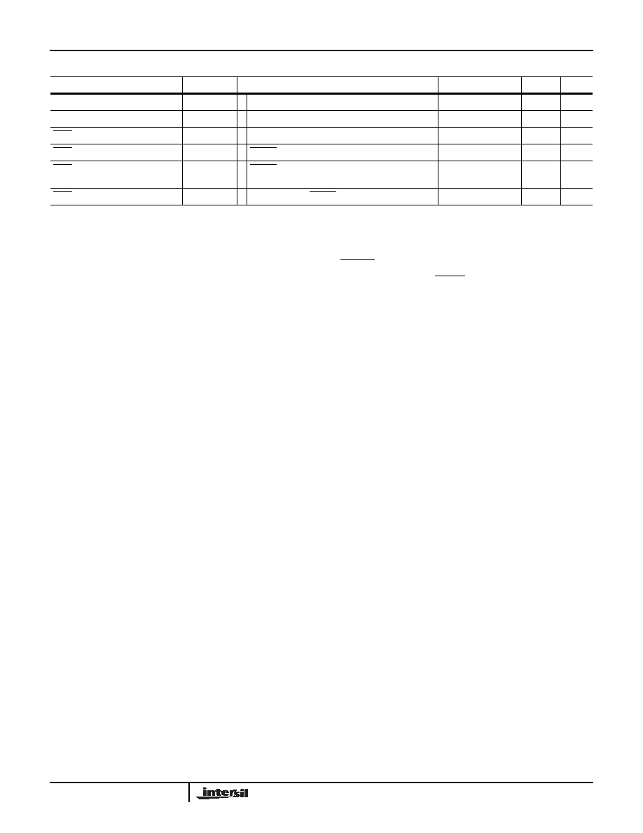
HVREF Voltage (VIN-HVREF)
HVREF(VZ)VIN = 10V to 75V
-
5.5
-
V
VSET Voltage (VOUT-VSET)
VREF(VSET)
VIN = 10V to 75V
-
5.3
-
V
Fault Low Output Voltage
VFLT_L
VIN - VOUT < 0V, VGATE = VGL
--
0.5
V
Fault Sink Current
IFLT_SINK
FAULT = VFLT_L, VIN < VOUT, VGATE = VGL
4-
-
mA
Fault Leakage Current
IFLT_LEAK
FAULT = ”VFLT_H”, VIN >VOUT, VGATE = VIN +
VGQP
-
10
A
Fault Delay -Low to High
TFLT
GATE = VGL to FAULT = VFLT_L
-
120
-
s
NOTES:
5. The * denotes parameters which are guaranteed by design and not production tested.
6. Specifications to +105°C and -40°C are guaranteed by design and not production tested.
Electrical Specifications
VIN = 48V, TA = -40
oC to 105oC, Unless Otherwise Specified (Continued)
PARAMETER
SYMBOL
TEST CONDITIONS
MIN
TYP
MAX
UNITS
ISL6144
相关PDF资料 |
PDF描述 |
|---|---|
| ISL6208CB | High Voltage Synchronous Rectified Buck MOSFET Driver |
| ISL6208CB-T | High Voltage Synchronous Rectified Buck MOSFET Driver |
| ISL6208CBZ | High Voltage Synchronous Rectified Buck MOSFET Driver |
| ISL6208CBZ-T | High Voltage Synchronous Rectified Buck MOSFET Driver |
| ISL6227CA | Dual Mobile-Friendly PWM Controller with DDR Option |
相关代理商/技术参数 |
参数描述 |
|---|---|
| ISL6144_07 | 制造商:INTERSIL 制造商全称:Intersil Corporation 功能描述:High Voltage ORing MOSFET Controller |
| ISL6144EVAL1 | 功能描述:EVALUATION BOARD ISL6144 ORING RoHS:否 类别:编程器,开发系统 >> 评估演示板和套件 系列:- 产品培训模块:Obsolescence Mitigation Program 标准包装:1 系列:- 主要目的:电源管理,电池充电器 嵌入式:否 已用 IC / 零件:MAX8903A 主要属性:1 芯锂离子电池 次要属性:状态 LED 已供物品:板 |
| ISL6144EVAL1Z | 功能描述:EVALUATION BOARD ISL6144 ORING RoHS:是 类别:编程器,开发系统 >> 评估演示板和套件 系列:- 标准包装:1 系列:PCI Express® (PCIe) 主要目的:接口,收发器,PCI Express 嵌入式:- 已用 IC / 零件:DS80PCI800 主要属性:- 次要属性:- 已供物品:板 |
| ISL6144IR | 功能描述:IC CTRLR MOSFET HV ORING 20-QFN RoHS:否 类别:集成电路 (IC) >> PMIC - O 圈控制器 系列:- 标准包装:1,000 系列:- 应用:电池备份,工业/汽车,大电流开关 FET 型:- 输出数:5 内部开关:是 延迟时间 - 开启:100ns 延迟时间 - 关闭:- 电源电压:3 V ~ 5.5 V 电流 - 电源:250µA 工作温度:0°C ~ 70°C 安装类型:表面贴装 封装/外壳:16-SOIC(0.154",3.90mm 宽) 供应商设备封装:16-SOIC N 包装:带卷 (TR) |
| ISL6144IR-T | 功能描述:IC CTRLR MOSFET HV ORING 20-QFN RoHS:否 类别:集成电路 (IC) >> PMIC - O 圈控制器 系列:- 标准包装:1,000 系列:- 应用:电池备份,工业/汽车,大电流开关 FET 型:- 输出数:5 内部开关:是 延迟时间 - 开启:100ns 延迟时间 - 关闭:- 电源电压:3 V ~ 5.5 V 电流 - 电源:250µA 工作温度:0°C ~ 70°C 安装类型:表面贴装 封装/外壳:16-SOIC(0.154",3.90mm 宽) 供应商设备封装:16-SOIC N 包装:带卷 (TR) |
发布紧急采购,3分钟左右您将得到回复。