- 您现在的位置:买卖IC网 > PDF目录176103 > ISL6144 (Intersil Corporation) High Voltage ORing MOSFET Controller PDF资料下载
参数资料
| 型号: | ISL6144 |
| 厂商: | Intersil Corporation |
| 英文描述: | High Voltage ORing MOSFET Controller |
| 中文描述: | 高电压的ORing MOSFET控制器 |
| 文件页数: | 12/14页 |
| 文件大小: | 404K |
| 代理商: | ISL6144 |
7
The slow turn off is achieved in two stages. The first stage
starts with a slow turn off action and lasts for up to 20s. The
gate pull down current for the first stage is 2mA. The second
slow turn off stage completes the gate turn off with a 10mA
pull down current. The 20s delay filters out any false trip off
due to noise or glitches that might be present on the supply
line.
The gate turn on and gate turn off drivers have a 50kHz filter
to reduce the variation in FET forward voltage drop (and FET
gate voltage) due to normal SMPS system switching noises
(typically higher than 50kHz). These filters do not affect the
total turn on or slow turn off times.
Special system design precautions must be taken to insure
that no AC mains related low frequency noise will be present
at the input or output of ISL6144. Filters and multiple power
conversion stages, which are part of any distributed dc
power system, normally filter out all such noise.
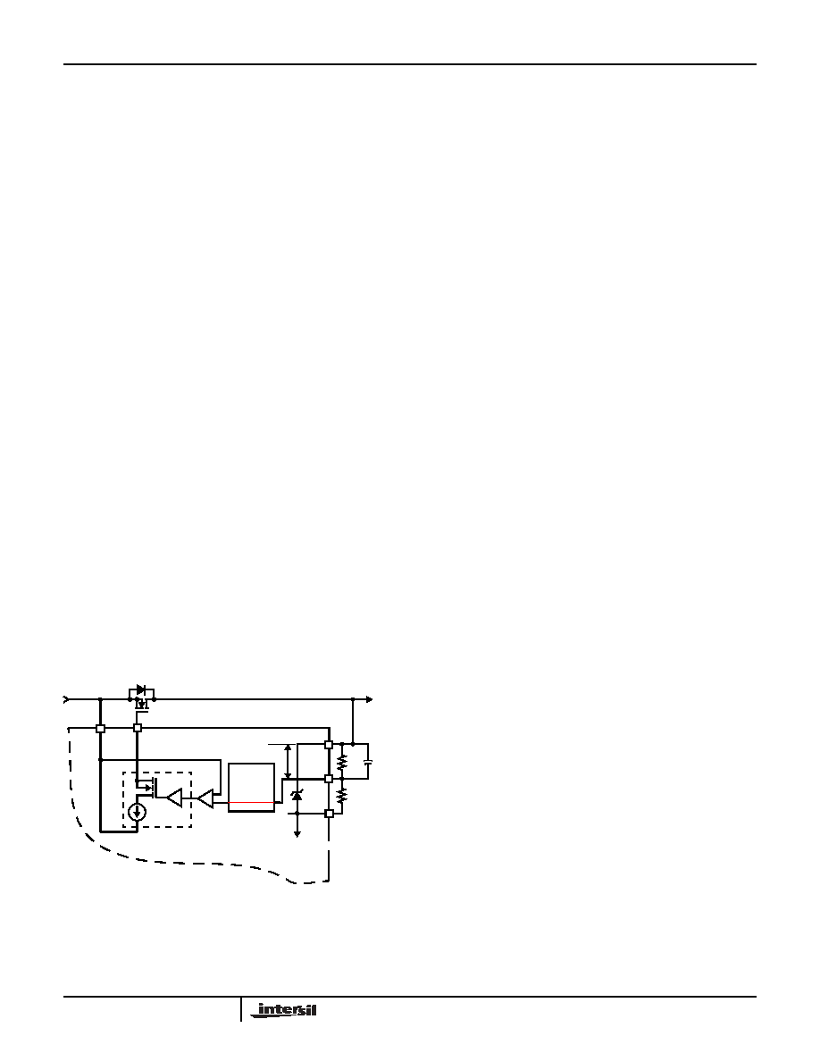
HS Comparator - Fast Turn Off
There is a High Speed (HS) Comparator used for fast turn-
off of the ORing MOSFET to protect the common bus
against hard short faults at a sourcing power supply output
(refer to Figure 3).
During normal operation the gate of the ORing MOSFET is
charge pumped to a voltage that depends on whether it is in
the 20mV regulation mode or fully enhanced. In this case:
If a dead short fault occurs in the sourcing supply, it causes
VIN to drop very quickly while VOUT is not affected as more
than one supply are paralleled. In the absence of the
ISL6144 functionality, a very high reverse current will flow
from Output to the Input supply pulling down the common
DC Bus, resulting in an overall “catastrophic” system failure.
The fault can be detected and isolated by using the ISL6144
and an N-channel ORing MOSFET. VIN is compared to
VCOMP, and whenever:
The fast turn off mechanism will be activated and the
MOSFET(s) will be turned off very quickly. The speed of this
turn off depends on the amount of equivalent gate loading
capacitance. For an equivalent Cgs = 39nF. The gate turn
off time is <300ns and gate pull down current is 2A.
The level of VTH(HS) (HS Comparator trip level) is adjustable
by means of external resistors R1 and R2 to a value
theoretically ranging from 0-5.3V. Typical values are 0.05V
to 0.3V. This is done in order to avoid false turn off due to
noise or minor glitches present in the DC switching power
supply. The threshold voltage is calculated as:
Where VREF(VSET) is an internal zener reference (5.3V
typical) between VOUT and VSET pins. R1 and R2 must be
chosen such that their sum is about 50k
. An external
capacitor C2 is needed between VOUT and COMP pins to
provide high frequency decoupling. The HS comparator has
an internal delay time on the order of 50ns which is part of
the <300ns overall turn off time specification (with
Cgs=39nF).
Gate Logic and Charge Pump
The IC has two charge pumps:
The first charge pump generates the floating gate drive for
the N-channel MOSFET. The second charge pump output
current opposes the pull down current of the slow turn off
transistor to provide regulation of the GATE voltage.
The presence of the charge pump allows the use of an
N-channel MOSFET with a floating gate drive. The
N-channel MOSFETs normally have lower rDS(ON) (not to
mention cost saving) compared to P-Channel MOSFETs,
allowing further reduction of conduction losses.
BIAS & REF
Bias currents for the two internal zener supplies (HVREF
and VSET) is provided by this block. This block also
provides a 0.6V band-gap reference used in the UV
detection circuit.
Undervoltage Comparator
The undervoltage comparator compares HVREF to 0.6V
internal reference. Once it falls below this level the UV
circuitry pulls and holds down the gate pin as long as the
HVREF UV condition is present. Voltage at both VIN and
HVREF pins track each other.
V
OUT
V
IN
I
OUT
–
r
DS(ON
)
=
(EQ. 1)
FIGURE 3. HS COMPARATOR
-
+
HV PASS
VOUT
COMP
VSET
GATE
VIN
HS
2A*
VIN
DRIVER
BIAS
CLAMP
&
VTH(HS)
5.3V
R1
R2
C2
SOURCING
SUPPLY
TO SHARED
LOAD
COMP
FROM
R1 + R2 = 50k
VIN VCOMP
<
VCOMP VOUT VTH HS
()
–
=
where
;
VTH(HS) is defined below
;
(EQ. 2)
V
TH HS
()
R1
R2
+
()
---------------------------V
REF VSET
()
=
(EQ. 3)
ISL6144
相关PDF资料 |
PDF描述 |
|---|---|
| ISL6208CB | High Voltage Synchronous Rectified Buck MOSFET Driver |
| ISL6208CB-T | High Voltage Synchronous Rectified Buck MOSFET Driver |
| ISL6208CBZ | High Voltage Synchronous Rectified Buck MOSFET Driver |
| ISL6208CBZ-T | High Voltage Synchronous Rectified Buck MOSFET Driver |
| ISL6227CA | Dual Mobile-Friendly PWM Controller with DDR Option |
相关代理商/技术参数 |
参数描述 |
|---|---|
| ISL6144_07 | 制造商:INTERSIL 制造商全称:Intersil Corporation 功能描述:High Voltage ORing MOSFET Controller |
| ISL6144EVAL1 | 功能描述:EVALUATION BOARD ISL6144 ORING RoHS:否 类别:编程器,开发系统 >> 评估演示板和套件 系列:- 产品培训模块:Obsolescence Mitigation Program 标准包装:1 系列:- 主要目的:电源管理,电池充电器 嵌入式:否 已用 IC / 零件:MAX8903A 主要属性:1 芯锂离子电池 次要属性:状态 LED 已供物品:板 |
| ISL6144EVAL1Z | 功能描述:EVALUATION BOARD ISL6144 ORING RoHS:是 类别:编程器,开发系统 >> 评估演示板和套件 系列:- 标准包装:1 系列:PCI Express® (PCIe) 主要目的:接口,收发器,PCI Express 嵌入式:- 已用 IC / 零件:DS80PCI800 主要属性:- 次要属性:- 已供物品:板 |
| ISL6144IR | 功能描述:IC CTRLR MOSFET HV ORING 20-QFN RoHS:否 类别:集成电路 (IC) >> PMIC - O 圈控制器 系列:- 标准包装:1,000 系列:- 应用:电池备份,工业/汽车,大电流开关 FET 型:- 输出数:5 内部开关:是 延迟时间 - 开启:100ns 延迟时间 - 关闭:- 电源电压:3 V ~ 5.5 V 电流 - 电源:250µA 工作温度:0°C ~ 70°C 安装类型:表面贴装 封装/外壳:16-SOIC(0.154",3.90mm 宽) 供应商设备封装:16-SOIC N 包装:带卷 (TR) |
| ISL6144IR-T | 功能描述:IC CTRLR MOSFET HV ORING 20-QFN RoHS:否 类别:集成电路 (IC) >> PMIC - O 圈控制器 系列:- 标准包装:1,000 系列:- 应用:电池备份,工业/汽车,大电流开关 FET 型:- 输出数:5 内部开关:是 延迟时间 - 开启:100ns 延迟时间 - 关闭:- 电源电压:3 V ~ 5.5 V 电流 - 电源:250µA 工作温度:0°C ~ 70°C 安装类型:表面贴装 封装/外壳:16-SOIC(0.154",3.90mm 宽) 供应商设备封装:16-SOIC N 包装:带卷 (TR) |
发布紧急采购,3分钟左右您将得到回复。