- 您现在的位置:买卖IC网 > PDF目录16359 > ISL6144EVAL1Z (Intersil)EVALUATION BOARD ISL6144 ORING PDF资料下载
参数资料
| 型号: | ISL6144EVAL1Z |
| 厂商: | Intersil |
| 文件页数: | 7/30页 |
| 文件大小: | 0K |
| 描述: | EVALUATION BOARD ISL6144 ORING |
| 标准包装: | 1 |
| 主要目的: | 电源管理,O 环控制器/负荷分载 |
| 已用 IC / 零件: | ISL6144 |
| 已供物品: | 板 |
第1页第2页第3页第4页第5页第6页当前第7页第8页第9页第10页第11页第12页第13页第14页第15页第16页第17页第18页第19页第20页第21页第22页第23页第24页第25页第26页第27页第28页第29页第30页
�� �
�
�ISL6144�
�The� slow� turn-off� is� achieved� in� two� stages.� The� first� stage�
�starts� with� a� slow� turn-off� action� and� lasts� for� up� to� 20μs.� The�
�gate� pull� down� current� for� the� first� stage� is� 2mA.� The� second�
�slow� turn-off� stage� completes� the� gate� turn-off� with� a� 10mA�
�pull� down� current.� The� 20μs� delay� filters� out� any� false� trip� off�
�The� fault� can� be� detected� and� isolated� by� using� the� ISL6144�
�and� an� N-Channel� ORing� MOSFET.� V� IN� is� compared� to�
�V� COMP� ,� and� whenever:�
�V� IN� <� V� COMP� ;� where�
�due� to� noise� or� glitches� that� might� be� present� on� the� supply�
�line.�
�The� gate� turn-on� and� gate� turn-off� drivers� have� a� 50kHz� filter�
�V� COMP� =� V� OUT� –� V� TH� (� HS� )�
�V� TH(HS)� is� defined� below�
�(EQ.� 2)�
�V� TH� (� HS� )� =� --------------------------� V� REF� (� VSET� )�
�(� R� 1� +� R� 2� )�
�V� OUT� =� V� IN� –� I� OUT� ?� r� DS(ON� )�
�to� reduce� the� variation� in� FET� forward� voltage� drop� (and� FET�
�gate� voltage)� due� to� normal� SMPS� system� switching� noises�
�(typically� higher� than� 50kHz).� These� filters� do� not� affect� the�
�total� turn-on� or� slow� turn-off� times.�
�Special� system� design� precautions� must� be� taken� to� insure�
�that� no� AC� mains� related� low� frequency� noise� will� be� present�
�at� the� input� or� output� of� ISL6144.� Filters� and� multiple� power�
�conversion� stages,� which� are� part� of� any� distributed� DC�
�power� system,� normally� filter� out� all� such� noise.�
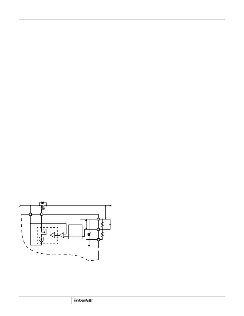
�HS� Comparator-Fast� Turn-off�
�There� is� a� High� Speed� (HS)� Comparator� used� for� fast� turn-�
�off� of� the� ORing� MOSFET� to� protect� the� common� bus�
�against� hard� short� faults� at� a� sourcing� power� supply� output�
�(refer� to� Figure� 1).�
�During� normal� operation� the� gate� of� the� ORing� MOSFET� is�
�charge� pumped� to� a� voltage� that� depends� on� whether� it� is� in�
�the� 20mV� regulation� mode� or� fully� enhanced.� In� this� case:�
�(EQ.� 1)�
�If� a� dead� short� fault� occurs� in� the� sourcing� supply,� it� causes�
�V� IN� to� drop� very� quickly� while� V� OUT� is� not� affected� as� more�
�than� one� supply� are� paralleled.� In� the� absence� of� the�
�ISL6144� functionality,� a� very� high� reverse� current� will� flow�
�from� Output� to� the� Input� supply� pulling� down� the� common�
�DC� Bus,� resulting� in� an� overall� “catastrophic”� system� failure.�
�FROM�
�SOURCING� TO� SHARED�
�SUPPLY� LOAD�
�The� fast� turn-off� mechanism� will� be� activated� and� the�
�MOSFET(s)� will� be� turned� off� very� quickly.� The� speed� of� this�
�turn-off� depends� on� the� amount� of� equivalent� gate� loading�
�capacitance.� For� an� equivalent� Cgs� =� 39nF.� The� gate� turn-off�
�time� is� <300ns� and� gate� pull� down� current� is� 2A.�
�The� level� of� V� TH(HS)� (HS� Comparator� trip� level)� is� adjustable�
�by� means� of� external� resistors� R� 1� and� R� 2� to� a� value�
�theoretically� ranging� from� 0V� to� 5.3V.� Typical� values� are�
�0.05V� to� 0.3V.� This� is� done� in� order� to� avoid� false� turn-off�
�due� to� noise� or� minor� glitches� present� in� the� DC� switching�
�power� supply.� The� threshold� voltage� is� calculated� as�
�Equation� 3:�
�R� 1�
�(EQ.� 3)�
�Where� V� REF(VSET)� is� an� internal� zener� reference� (5.3V�
�typical)� between� V� OUT� and� VSET� pins.� R� 1� and� R� 2� must� be�
�chosen� such� that� their� sum� is� about� 50k� Ω� .� An� external�
�capacitor,� C� 2� ,� is� needed� between� V� OUT� and� COMP� pins� to�
�provide� high� frequency� decoupling.� The� HS� comparator� has�
�an� internal� delay� time� on� the� order� of� 50ns,� which� is� part� of�
�the� <300ns� overall� turn-off� time� specification� (with�
�Cgs� =� 39nF).�
�Gate� Logic� and� Charge� Pump�
�The� IC� has� two� charge� pumps.� The� first� charge� pump�
�generates� the� floating� gate� drive� for� the� N-Channel�
�MOSFET.� The� second� charge� pump� output� current� opposes�
�the� pull� down� current� of� the� slow� turn-off� transistor� to� provide�
�regulation� of� the� GATE� voltage.�
�The� presence� of� the� charge� pump� allows� the� use� of� an�
�+�
�HV� PASS�
�VIN�
�GATE�
�VIN�
�-�
�2A*�
�HS�
�DRIVER� COMP�
�VOUT�
�V� TH(HS)�
�COMP�
�AND�
�CLAMP�
�5.3V� VSET�
�BIAS�
�R� 1�
�R� 2�
�C� 2�
�N-Channel� MOSFET� with� a� floating� gate� drive.� The�
�N-Channel� MOSFETs� normally� have� lower� r� DS(ON)� (not� to�
�mention� cost� saving)� compared� to� P-Channel� MOSFETs,�
�allowing� further� reduction� of� conduction� losses.�
�BIAS� and� REF�
�Bias� currents� for� the� two� internal� zener� supplies� (HVREF�
�FIGURE� 1.� HS� COMPARATOR�
�7�
�R� 1� + R� 2� = 50k� Ω�
�and� VSET)� is� provided� by� this� block.� This� block� also�
�provides� a� 0.6V� band-gap� reference� used� in� the� UV�
�detection� circuit.�
�Undervoltage� Comparator�
�The� undervoltage� comparator� compares� HVREF� to� 0.6V�
�internal� reference.� Once� it� falls� below� this� level� the� UV�
�circuitry� pulls� and� holds� down� the� gate� pin� as� long� as� the�
�HVREF� UV� condition� is� present.� Voltage� at� both� VIN� and�
�HVREF� pins� track� each� other.�
�FN9131.7�
�October� 6,� 2011�
�相关PDF资料 |
PDF描述 |
|---|---|
| LK1005R18K-T | INDUCTOR MULTILAYER .18UH 0402 |
| LK1005R15K-T | INDUCTOR MULTILAYER .15UH 0402 |
| A3BKB-2006G | IDC CABLE- ASR20B/AE20G/APK20B |
| LK1005R12K-T | INDUCTOR MULTILAYER .12UH 0402 |
| H1KXH-6036G | IDC CABLE - HPK60H/AE60G/X |
相关代理商/技术参数 |
参数描述 |
|---|---|
| ISL6144IR | 功能描述:IC CTRLR MOSFET HV ORING 20-QFN RoHS:否 类别:集成电路 (IC) >> PMIC - O 圈控制器 系列:- 标准包装:1,000 系列:- 应用:电池备份,工业/汽车,大电流开关 FET 型:- 输出数:5 内部开关:是 延迟时间 - 开启:100ns 延迟时间 - 关闭:- 电源电压:3 V ~ 5.5 V 电流 - 电源:250µA 工作温度:0°C ~ 70°C 安装类型:表面贴装 封装/外壳:16-SOIC(0.154",3.90mm 宽) 供应商设备封装:16-SOIC N 包装:带卷 (TR) |
| ISL6144IR-T | 功能描述:IC CTRLR MOSFET HV ORING 20-QFN RoHS:否 类别:集成电路 (IC) >> PMIC - O 圈控制器 系列:- 标准包装:1,000 系列:- 应用:电池备份,工业/汽车,大电流开关 FET 型:- 输出数:5 内部开关:是 延迟时间 - 开启:100ns 延迟时间 - 关闭:- 电源电压:3 V ~ 5.5 V 电流 - 电源:250µA 工作温度:0°C ~ 70°C 安装类型:表面贴装 封装/外壳:16-SOIC(0.154",3.90mm 宽) 供应商设备封装:16-SOIC N 包装:带卷 (TR) |
| ISL6144IRZA | 功能描述:热插拔功率分布 W/ANNEAL 20LD 5X5 QF N ORING FET CONTRLR RoHS:否 制造商:Texas Instruments 产品:Controllers & Switches 电流限制: 电源电压-最大:7 V 电源电压-最小:- 0.3 V 工作温度范围: 功率耗散: 安装风格:SMD/SMT 封装 / 箱体:MSOP-8 封装:Tube |
| ISL6144IRZA-T | 功能描述:IC CTRLR MOSFET HV ORING 20-QFN RoHS:是 类别:集成电路 (IC) >> PMIC - O 圈控制器 系列:- 标准包装:1,000 系列:- 应用:电池备份,工业/汽车,大电流开关 FET 型:- 输出数:5 内部开关:是 延迟时间 - 开启:100ns 延迟时间 - 关闭:- 电源电压:3 V ~ 5.5 V 电流 - 电源:250µA 工作温度:0°C ~ 70°C 安装类型:表面贴装 封装/外壳:16-SOIC(0.154",3.90mm 宽) 供应商设备封装:16-SOIC N 包装:带卷 (TR) |
| ISL6144IV | 功能描述:IC CTRLR MOSFET ORING HV 16TSSOP RoHS:否 类别:集成电路 (IC) >> PMIC - O 圈控制器 系列:- 标准包装:1,000 系列:- 应用:电池备份,工业/汽车,大电流开关 FET 型:- 输出数:5 内部开关:是 延迟时间 - 开启:100ns 延迟时间 - 关闭:- 电源电压:3 V ~ 5.5 V 电流 - 电源:250µA 工作温度:0°C ~ 70°C 安装类型:表面贴装 封装/外壳:16-SOIC(0.154",3.90mm 宽) 供应商设备封装:16-SOIC N 包装:带卷 (TR) |
发布紧急采购,3分钟左右您将得到回复。