- 您现在的位置:买卖IC网 > PDF目录20329 > ISL6144IVZA-T (Intersil)IC CTRLR MOSFET HV ORING 16TSSOP PDF资料下载
参数资料
| 型号: | ISL6144IVZA-T |
| 厂商: | Intersil |
| 文件页数: | 6/30页 |
| 文件大小: | 0K |
| 描述: | IC CTRLR MOSFET HV ORING 16TSSOP |
| 标准包装: | 2,500 |
| 应用: | 电信/数据通信系统 |
| FET 型: | N 沟道 |
| 输出数: | 1 |
| 内部开关: | 无 |
| 延迟时间 - 开启: | 1ms |
| 延迟时间 - 关闭: | 250ns |
| 电源电压: | 9 V ~ 75 V |
| 工作温度: | -40°C ~ 105°C |
| 安装类型: | 表面贴装 |
| 封装/外壳: | 16-TSSOP(0.173",4.40mm 宽) |
| 供应商设备封装: | 16-TSSOP |
| 包装: | 带卷 (TR) |
第1页第2页第3页第4页第5页当前第6页第7页第8页第9页第10页第11页第12页第13页第14页第15页第16页第17页第18页第19页第20页第21页第22页第23页第24页第25页第26页第27页第28页第29页第30页
�� �
�
�ISL6144�
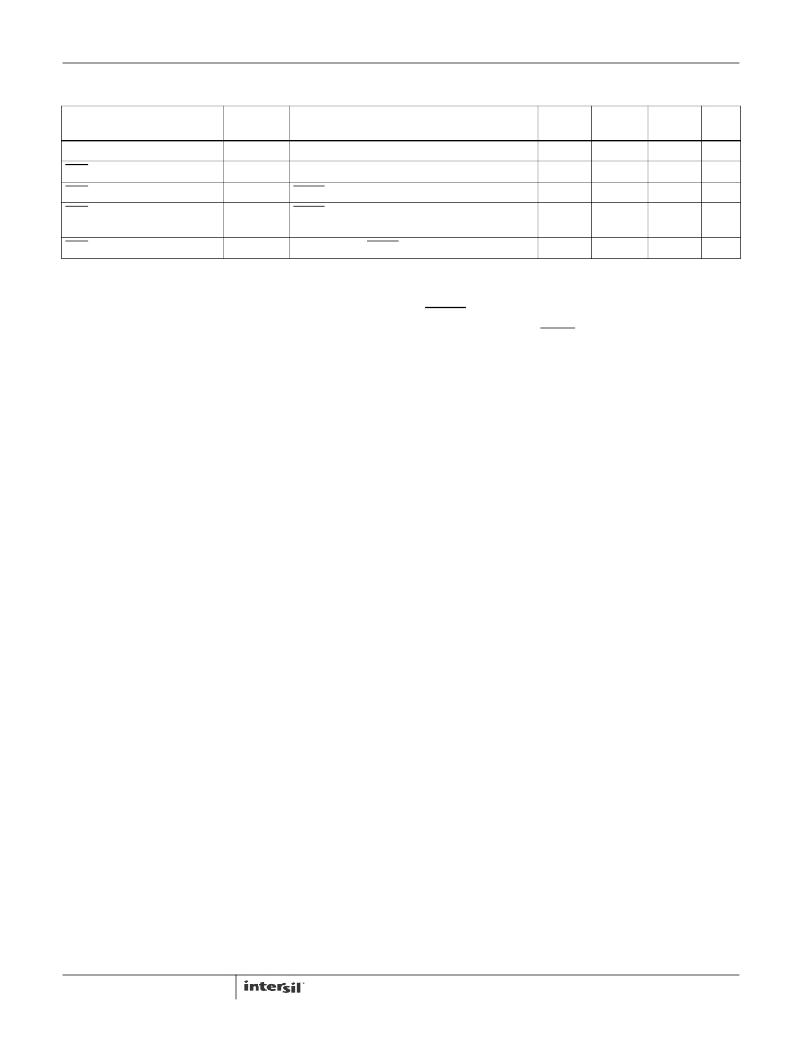
�Electrical� Specifications�
�V� IN� =� 48V,� T� A� =� -40°C� to� +105°C,� Unless� Otherwise� Specified.� Boldface� limits� apply� over� the� operating�
�temperature� range,� -40°C� to� +105°C.�
�MIN�
�MAX�
�PARAMETER�
�SYMBOL�
�TEST� CONDITIONS�
�(Note� 12)�
�TYP�
�(Note� 12)� UNITS�
�VSET� Voltage� (V� OUT� -� VSET)�
�V� REF(VSET)� V� IN� =� 9V� to� 75V�
�-�
�5.3�
�-�
�V�
�Fault� Low� Output� Voltage�
�Fault� Sink� Current�
�Fault� Leakage� Current�
�Fault� Delay� -� Low� to� High�
�V� FLT_L�
�I� FLT_SINK�
�I� FLT_LEAK�
�t� FLT�
�V� IN� -� V� OUT� <� 0V,� V� GATE� =� V� GL�
�FAULT� =� V� FLT_L� ,� V� IN� <� V� OUT� ,� V� GATE� =� V� GL�
�FAULT� =� ”V� FLT_H� ”,� V� IN� >� V� OUT� ,� V� GATE� =� V� IN� +�
�V� GQP�
�GATE� =� V� GL� to� FAULT� =� V� FLT_L�
�-�
�4�
�-�
�-�
�-�
�-�
�-�
�120�
�0.5�
�-�
�10�
�-�
�V�
�mA�
�μA�
�μs�
�NOTES:�
�12.� Compliance� to� datasheet� limits� is� assured� by� one� or� more� methods:� production� test,� characterization� and/or� design.�
�Functional� Pin� Descriptions�
�GATE�
�This� is� the� Gate� Drive� output� of� the� external� N-Channel�
�MOSFET� generated� by� the� IC� internal� charge� pump.� Gate�
�turn-on� time� is� typically� 1ms.�
�VIN�
�Input� bias� pin� connected� to� the� sourcing� supply� side� (ORing�
�MOSFET� Source).� Also� serves� as� the� sense� pin� to�
�determine� the� sourcing� supply� voltage.� The� ORing� MOSFET�
�will� be� turned� off� when� VIN� becomes� lower� than� VOUT� by� a�
�value� more� than� the� externally� set� threshold.�
�VOUT�
�Connected� to� the� Load� side� (ORing� MOSFET� Drain).� This� is�
�the� VOUT� sense� pin� connected� to� the� load.� This� is� the�
�common� connection� point� for� multiple� paralleled� supplies.�
�VOUT� is� compared� to� VIN� to� determine� when� the� ORing�
�FET� has� to� be� turned� off.�
�HVREF�
�Low� side� of� the� internal� IC� High� Voltage� Reference� used� by�
�internal� circuitry,� also� available� as� an� external� pin� for�
�additional� external� capacitor� connection.�
�COMP�
�This� is� the� high� side� connection� for� the� HS� Comparator� trip�
�level� setting� (V� TH(HS)� ).� Resistor� R� 1� ,� connected� between�
�COMP� and� V� OUT� along� with� resistor� R� 2� ,� provides� adjustable�
�V� OUT� -� V� IN� trip� level� (0V� to� 5V).� This� provides� flexibility� to�
�externally� set� the� desired� level� depending� on� particular�
�system� requirement.�
�VSET�
�Low� side� connection� for� the� HS� Comparator� trip� level� setting�
�A� second� resistor� R� 2� connected� between� VSET� and� COMP�
�provides� adjustable� “V� IN� -� V� OUT� ”� level� along� with� R� 1� .�
�6�
�FAULT�
�Open-Drain� pull-down� FAULT� Output� with� internal� on-chip�
�filtering� (� t� FLT� ).� The� ISL6144� fault� detection� circuitry� will�
�pull-down� this� pin� to� GND� as� soon� as� it� detects� a� fault.�
�Different� types� of� faults� and� their� detection� mechanisms� are�
���GND�
�IC� ground� reference.�
�Detailed� Description�
�The� ISL6144� and� a� suitably� sized� N-Channel� power�
�MOSFET(s)� increases� power� distribution� efficiency� and�
�availability� when� replacing� a� power� ORing� diode� in� high� current�
��for� power� saving� when� using� ISL6144� with� an� N-channel� ORing�
�MOSFET� compared� to� a� typical� ORing� diode.�
�Functional� Block� Description�
�Regulating� Amplifier-Slow� (Quiet)� Turn-off�
�A� Hysteretic� Regulating� (HR)� Amplifier� is� used� for� a�
�Quiet/Slow� turn-off� mechanism.� This� slow� turn-off� is� initiated�
�when� the� sourcing� power� supply� is� turned� off� slowly� for�
�system� diagnostics.� Under� normal� operating� conditions� as�
�V� OUT� pulls� up� to� 20mV� below� V� IN� (V� IN� -� 20mV� >� V� OUT� ),� the�
�HR� Amplifier� regulates� the� gate� voltage� to� keep� the� 20mV�
�(� V� FWD_HR� )� forward� voltage� drop� across� the� ORing� MOSFET�
�(Vs� -� Vd).� This� will� continue� until� the� load� current� exceeds�
�the� MOSFET� ability� to� deliver� the� current� with� Vsd� of� 20mV.�
�In� this� case,� Gate� will� be� charged� to� the� full� charge� pump�
�voltage� (V� GQP� )� to� fully� enhance� the� MOSFET.� At� this� point,�
�the� MOSFET� will� be� fully� enhanced� and� behave� as� a�
�constant� resistor� valued� at� the� r� DS(ON)� .� Once� V� IN� starts� to�
�drop� below� V� OUT� ,� regulation� cannot� be� maintained� and� the�
�output� of� the� HR� Amp� is� pulled� high� and� the� gate� is� pulled�
�down� to� V� IN� slowly� in� less� than� a� 100μs.� As� a� result,� the�
�ORing� FET� is� turned� off,� avoiding� reverse� current� as� well� as�
�voltage� and� current� stresses� on� supply� components.�
�FN9131.7�
�October� 6,� 2011�
�相关PDF资料 |
PDF描述 |
|---|---|
| EBM12DTAD-S189 | CONN EDGECARD 24POS R/A .156 SLD |
| EBM06DSAI | CONN EDGECARD 12POS R/A .156 SLD |
| HBM08DRYN-S13 | CONN EDGECARD 16POS .156 EXTEND |
| A470K15C0GL5TAA | CAP CER 47PF 500V 10% NP0 AXIAL |
| T95D227K010LSAS | CAP TANT 220UF 10V 10% 2917 |
相关代理商/技术参数 |
参数描述 |
|---|---|
| ISL6144IVZA-T7A | 功能描述:热插拔功率分布 W/ANNEAL 16LD TSSOP ORING FET CONTRLR RoHS:否 制造商:Texas Instruments 产品:Controllers & Switches 电流限制: 电源电压-最大:7 V 电源电压-最小:- 0.3 V 工作温度范围: 功率耗散: 安装风格:SMD/SMT 封装 / 箱体:MSOP-8 封装:Tube |
| ISL6146 | 制造商:INTERSIL 制造商全称:Intersil Corporation 功能描述:Low Voltage ORing FET Controller |
| ISL6146A | 制造商:INTERSIL 制造商全称:Intersil Corporation 功能描述:Low Voltage ORing FET Controller |
| ISL6146AEVAL1Z | 制造商:Intersil Corporation 功能描述:ISL6146A EVALUATION BOARD - 8 LEAD - MSOP - ROHS COMPLIANT - Bulk 制造商:Intersil Corporation 功能描述:BOARD EVAL FOR ISL6146 制造商:Intersil 功能描述:ISL98002CRZ-EVALZ EVAL BRD RHS COMPLIA |
| ISL6146AFRZ | 功能描述:IC INTERFACE RoHS:是 类别:集成电路 (IC) >> PMIC - O 圈控制器 系列:* 标准包装:1,000 系列:- 应用:电池备份,工业/汽车,大电流开关 FET 型:- 输出数:5 内部开关:是 延迟时间 - 开启:100ns 延迟时间 - 关闭:- 电源电压:3 V ~ 5.5 V 电流 - 电源:250µA 工作温度:0°C ~ 70°C 安装类型:表面贴装 封装/外壳:16-SOIC(0.154",3.90mm 宽) 供应商设备封装:16-SOIC N 包装:带卷 (TR) |
发布紧急采购,3分钟左右您将得到回复。