- 您现在的位置:买卖IC网 > PDF目录383141 > ISL6173 (Intersil Corporation) Dual Low Voltage Hot Swap Controller PDF资料下载
参数资料
| 型号: | ISL6173 |
| 厂商: | Intersil Corporation |
| 元件分类: | 基准电压源/电流源 |
| 英文描述: | Dual Low Voltage Hot Swap Controller |
| 中文描述: | 双低电压热插拔控制器 |
| 文件页数: | 5/20页 |
| 文件大小: | 452K |
| 代理商: | ISL6173 |
5
FN9186.2
February 15, 2005
Absolute Maximum Ratings
Thermal Information
VBIAS . . . . . . . . . . . . . . . . . . . . . . . . . . . . . . . . . . . . . . . . . . . +5.5V
GTx, CPQ+ . . . . . . . . . . . . . . . . . . . . . . . . . . . . . . . . .-0.3V to +12V
ENx, RTR/LTCH, SNSx, PGx, FLTx, VSx, CTx, UVx,
SSx, CPQ-, CPVDD. . . . . . . . . . . . . . . . . . . . . . . . -0.3V to 5.5VDC
Output Current . . . . . . . . . . . . . . . . . . . . . . .Short Circuit Protected
ESD Rating
Human Body Model (Per MIL-STD-883 Method 3015.7). . .1750V
Machine Model (Per EIAJ ED-4701 Method C-111). . . . . . . .125V
Charged Device Model (Per EOS/ESD DS5.3, 4/14/93) . . .1750V
Operating Conditions
VBIAS/VIN1 Supply Voltage Range. . . . . . . . . . . .+2.25V to +3.63V
Temperature Range (T
A
) . . . . . . . . . . . . . . . . . . . . . . . . 0°C to 85°C
Thermal Resistance (Typical, Notes 1, 4)
5x5 QFN Package . . . . . . . . . . . . . . . .
Maximum Junction Temperature . . . . . . . . . . . . . . . . . . . . . . . .150°C
Maximum Storage Temperature Range. . . . . . . . . . .-65°C to 150°C
For recommended soldering conditions, see Tech Brief TB389.
(QFN - Leads Only)
θ
JA
(°C/W)
42
θ
JC
(°C/W)
12.5
CAUTION: Stresses above those listed in “Absolute Maximum Ratings” may cause permanent damage to the device. This is a stress only rating and operation of the
device at these or any other conditions above those indicated in the operational sections of this specification is not implied.
NOTES:
1.
θ
JA
is measured in free air with the component mounted on a high effective thermal conductivity test board with “direct attach” features. See
Tech Brief TB379.
2. All voltages are relative to GND, unless otherwise specified.
3. 1V (min) on the BIAS pin required for FLT to be valid.
4. For
θ
JC
, the “case temp” location is the center of the exposed metal pad on the package underside.
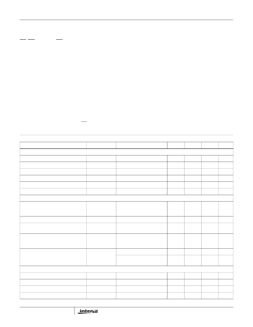
Electrical Specifications
V
DD
= 2.5V to +3.3V, T
A
= T
J
= 0°C - 85°C, Unless Otherwise Specified.
PARAMETER
SYMBOL
TEST CONDITIONS
MIN
TYP
MAX
UNIT
CURRENT REGULATION CONTROL
Current Regulation Threshold Voltage
V
CRVTH_1
RISET = 1.25K 1%, I
SET
= 20μA
20
25
30
mV
Current Regulation Accuracy
V
CRVTH_1
R
RISET = 1.25K 1%, I
SET
= 20μA
-20
+20
%
Current Regulation Threshold Voltage
V
CRVTH_2
RISET = 2.50K 1%, I
SET
= 20μA
45
50
55
mV
Current Regulation Accuracy
V
CRVTH_2
R
RISET = 2.50K 1%, I
SET
= 20μA
-10
+10
%
CT Threshold Voltage
V
CT_Vth
1.128
1.178
1.202
V
CT Charging Current
I
CT
10
μ
A
GATE DRIVE
GATE Response Time from WOC (Open)
pd_woc_open
GATE open
100mV of overdrive on the WOC
comparator
3
ns
GATE Response Time from WOC (Loaded)
pd_woc_load
GATE = 1nF
100
ns
GATE Response Time in Current Regulation
mode (Loaded)
pd_cr_load
GATE = 1nF
120% Load Current
5
μs
GATE Turn-On Current
IGATE
GATE = 2V
V
VS
= 2V
V
SNS
= 2.1V
21
24
27
μA
GATE Voltage
V
GATE
Bias = 2.5V (see graph on page 7)
7.5
9.0
V
2.1 < Bias < 2.5
(see graph on page 7)
8
V
BIAS
Supply Current
I
BIAS
V
BIAS
= 3.3V
9
17
mA
POR Rising Threshold
VIN_POR_L2H
2.12
V
POR Falling Threshold
VIN_POR_H2L
2.10
V
POR Threshold Hysteresis
VIN_POR_HYS
5
mV
ISL6173
相关PDF资料 |
PDF描述 |
|---|---|
| ISL6173EVAL3 | Dual Low Voltage Hot Swap Controller |
| ISL6173DRZA-T | Dual Low Voltage Hot Swap Controller |
| ISL6206CB | High Voltage Synchronous Rectified Buck MOSFET Driver |
| ISL6206 | Octal D-Type Transparent Latches With 3-State Outputs 20-TSSOP -40 to 85 |
| ISL6206CB-T | High Voltage Synchronous Rectified Buck MOSFET Driver |
相关代理商/技术参数 |
参数描述 |
|---|---|
| ISL6173_06 | 制造商:INTERSIL 制造商全称:Intersil Corporation 功能描述:Dual Low Voltage Hot Swap Controller |
| ISL6173DRZA | 功能描述:IC CTRLR HOT SWAP DUAL LV 28QFN RoHS:是 类别:集成电路 (IC) >> PMIC - 热交换 系列:- 标准包装:50 系列:- 类型:热交换控制器 应用:-48V 远程电力系统,AdvancedTCA ? 系统,高可用性 内部开关:无 电流限制:可调 电源电压:11.5 V ~ 14.5 V 工作温度:-40°C ~ 85°C 安装类型:表面贴装 封装/外壳:10-TFSOP,10-MSOP(0.118",3.00mm 宽) 供应商设备封装:10-MSOP 包装:管件 |
| ISL6173DRZA-T | 功能描述:IC CTRLR HOT SWAP DUAL LV 28-QFN RoHS:是 类别:集成电路 (IC) >> PMIC - 热交换 系列:- 产品培训模块:Obsolescence Mitigation Program 标准包装:100 系列:- 类型:热插拔开关 应用:通用 内部开关:是 电流限制:可调 电源电压:9 V ~ 13.2 V 工作温度:-40°C ~ 150°C 安装类型:表面贴装 封装/外壳:10-WFDFN 裸露焊盘 供应商设备封装:10-TDFN-EP(3x3) 包装:管件 |
| ISL6173EVAL1 | 功能描述:EVALUATION BOARD FOR ISL6173 RoHS:否 类别:编程器,开发系统 >> 评估演示板和套件 系列:- 标准包装:1 系列:PCI Express® (PCIe) 主要目的:接口,收发器,PCI Express 嵌入式:- 已用 IC / 零件:DS80PCI800 主要属性:- 次要属性:- 已供物品:板 |
| ISL6173EVAL3 | 制造商:INTERSIL 制造商全称:Intersil Corporation 功能描述:Dual Low Voltage Hot Swap Controller |
发布紧急采购,3分钟左右您将得到回复。