- 您现在的位置:买卖IC网 > Datasheet目录333 > ISL6208CBZ-T (Intersil)IC MOSFET DRVR SYNC BUCK 8-SOIC Datasheet资料下载
参数资料
| 型号: | ISL6208CBZ-T |
| 厂商: | Intersil |
| 文件页数: | 8/13页 |
| 文件大小: | 0K |
| 描述: | IC MOSFET DRVR SYNC BUCK 8-SOIC |
| 标准包装: | 2,500 |
| 配置: | 高端和低端,同步 |
| 输入类型: | PWM |
| 延迟时间: | 20ns |
| 电流 - 峰: | 2A |
| 配置数: | 1 |
| 输出数: | 2 |
| 高端电压 - 最大(自引导启动): | 33V |
| 电源电压: | 4.5 V ~ 5.5 V |
| 工作温度: | -10°C ~ 100°C |
| 安装类型: | 表面贴装 |
| 封装/外壳: | 8-SOIC(0.154",3.90mm 宽) |
| 供应商设备封装: | 8-SOIC |
| 包装: | 带卷 (TR) |
�� �
�
�ISL6208,� ISL6208B�
�Diode� Emulation�
�Diode� emulation� allows� for� higher� converter� efficiency� under�
�light� load� situations.� With� diode� emulation� active,� the� ISL6208�
�will� detect� the� zero� current� crossing� of� the� output� inductor� and�
�turn� off� LGATE.� This� ensures� that� discontinuous� conduction�
�mode� (DCM)� is� achieved.� Diode� emulation� is� asynchronous� to�
�the� PWM� signal.� Therefore,� the� ISL6208� will� respond� to� the�
�FCCM� input� immediately� after� it� changes� state.� Refer�
�to“Typical� Performance� Waveforms”� on� page� 7.� NOTE:� Intersil�
�2.0�
�1.8�
�1.6�
�1.4�
�1.2�
�1.0�
�0.8�
�does� not� recommend� Diode� Emulation� use� with� r� DS(ON)�
�current� sensing� topologies.� The� turn-OFF� of� the� low� side�
�MOSFET� can� cause� gross� current� measurement� inaccuracies.�
�0.6�
�0.4�
�0.2�
�20nC�
�Q� GATE� = 100nC�
�Three-State� PWM� Input�
�0.0�
�0.0�
�0.1�
�0.2�
�0.3�
�0.4� 0.5� 0.6�
�0.7�
�0.8�
�0.9�
�1.0�
�P� =� f� sw� (� 1.5V� U� Q� +� V� L� Q� )� +� I� VCC� V�
�(EQ.� 2)�
�A� unique� feature� of� the� ISL6208� and� other� Intersil� drivers� is� the�
�addition� of� a� shutdown� window� to� the� PWM� input.� If� the� PWM�
�signal� enters� and� remains� within� the� shutdown� window� for� a� set�
�holdoff� time,� the� output� drivers� are� disabled� and� both� MOSFET�
�gates� are� pulled� and� held� low.� The� shutdown� state� is� removed�
�when� the� PWM� signal� moves� outside� the� shutdown� window.�
�Otherwise,� the� PWM� rising� and� falling� thresholds� outlined� in� the�
�“Electrical� Specifications”� table� on� page� 3� determine� when� the�
�lower� and� upper� gates� are� enabled.�
�Adaptive� Shoot-Through� Protection�
�Both� drivers� incorporate� adaptive� shoot-through� protection� to�
�prevent� upper� and� lower� MOSFETs� from� conducting�
�simultaneously� and� shorting� the� input� supply.� This� is�
�accomplished� by� ensuring� the� falling� gate� has� turned� off� one�
�MOSFET� before� the� other� is� allowed� to� turn� on.�
�During� turn-off� of� the� lower� MOSFET,� the� LGATE� voltage� is�
�monitored� until� it� reaches� a� 1V� threshold,� at� which� time� the�
�UGATE� is� released� to� rise.� Adaptive� shoot-through� circuitry�
�monitors� the� upper� MOSFET� gate-to-source� voltage� during� UGATE�
�turn-off.� Once� the� upper� MOSFET� gate-to-source� voltage� has�
�dropped� below� a� threshold� of� 1V,� the� LGATE� is� allowed� to� rise.�
�Internal� Bootstrap� Diode�
�This� driver� features� an� internal� bootstrap� Schottky� diode.�
�Simply� adding� an� external� capacitor� across� the� BOOT� and�
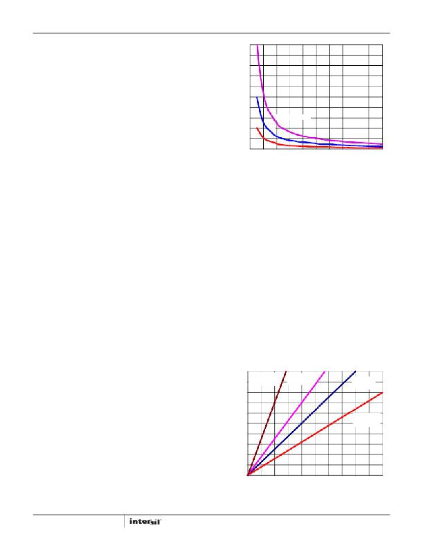
�Δ� V� BOOT_CAP� (V)�
�FIGURE� 8.� BOOTSTRAP� CAPACITANCE� vs� BOOT� RIPPLE�
�VOLTAGE�
�Power� Dissipation�
�Package� power� dissipation� is� mainly� a� function� of� the�
�switching� frequency� and� total� gate� charge� of� the� selected�
�MOSFETs.� Calculating� the� power� dissipation� in� the� driver� for� a�
�desired� application� is� critical� to� ensuring� safe� operation.�
�Exceeding� the� maximum� allowable� power� dissipation� level� will�
�push� the� IC� beyond� the� maximum� recommended� operating�
�junction� temperature� of� +125°C.� The� maximum� allowable� IC�
�power� dissipation� for� the� SO-8� package� is� approximately�
�800mW.� When� designing� the� driver� into� an� application,� it� is�
�recommended� that� the� following� calculation� be� performed� to�
�ensure� safe� operation� at� the� desired� frequency� for� the� selected�
�MOSFETs.� The� power� dissipated� by� the� driver� is� approximated�
�as� shown� in� Equation� 2:�
�U� L� CC�
�where� f� sw� is� the� switching� frequency� of� the� PWM� signal.� V� U�
�and� V� L� represent� the� upper� and� lower� gate� rail� voltage.� Q� U� and�
�Q� L� is� the� upper� and� lower� gate� charge� determined� by� MOSFET�
�selection� and� any� external� capacitance� added� to� the� gate� pins.�
�The� lV� CC� V� CC� product� is� the� quiescent� power� of� the� driver� and�
�is� typically� negligible.�
�C� BOOT� ≥� ---------------------�
�PHASE� pins� completes� the� bootstrap� circuit.�
�The� bootstrap� capacitor� must� have� a� maximum� voltage� rating�
�above� the� maximum� battery� voltage� plus� 5V.� The� bootstrap�
�capacitor� can� be� chosen� from� Equation� 1:�
�Q� GATE�
�(EQ.� 1)�
�Δ� V� BOOT�
�1000�
�900�
�800�
�700�
�600�
�Q� U� =100nC�
�Q� L� =� 200nC�
�Q� U� =� 50nC�
�Q� L� =� 100nC�
�Q� U� =� 50nC�
�Q� L� =� 50nC�
�Q� U� =� 20nC�
�500�
�Q� L� =50nC�
�where� Q� GATE� is� the� amount� of� gate� charge� required� to� fully�
�charge� the� gate� of� the� upper� MOSFET.� The� Δ� V� BOOT� term� is�
�defined� as� the� allowable� droop� in� the� rail� of� the� upper� drive.�
�As� an� example,� suppose� an� upper� MOSFET� has� a� gate� charge,�
�400�
�300�
�200�
�Q� GATE� ,� of� 25nC� at� 5V� and� also� assume� the� droop� in� the� drive�
�voltage� over� a� PWM� cycle� is� 200mV.� One� will� find� that� a�
�bootstrap� capacitance� of� at� least� 0.125μF� is� required.� The� next�
�larger� standard� value� capacitance� is� 0.15μF.� A� good� quality�
�100�
�0�
�0�
�200�
�400�
�600�
�800� 1000� 1200� 1400� 1600� 1800� 2000�
�FREQUENCY� (kHz)�
�ceramic� capacitor� is� recommended.�
�8�
�FIGURE� 9.� POWER� DISSIPATION� vs� FREQUENCY�
�FN9115.6�
�January� 31,� 2012�
�相关PDF资料 |
PDF描述 |
|---|---|
| ISL6209CB-T | IC MOSFET DRVR SYNC BUCK 8-SOIC |
| ISL6210CRZ | IC MOSFET DRIVER DUAL SYNC 16QFN |
| ISL6244EVAL1 | EVALUATION BOARD ISL6244 |
| ISL6261AEVAL1Z | EVAL BOARD 1 FOR ISL6261A |
| ISL6261EVAL1Z | EVAL BOARD FOR ISL6261 1 QFN |
相关代理商/技术参数 |
参数描述 |
|---|---|
| ISL6208CHRZ-T | 制造商:Intersil Corporation 功能描述:LEAD-FREE VERSION OF ISL6208CR - COST IMPROVEMENT - JAZZ FAB - Tape and Reel 制造商:Intersil Corporation 功能描述:IC MOSFET DRVR SYNC BUCK 8DFN |
| ISL6208CIRZ-T | 制造商:Intersil Corporation 功能描述:LEAD-FREE VERSION OF ISL6208CR - COST IMPROVEMENT - JAZZ FAB - Tape and Reel 制造商:Intersil Corporation 功能描述:IC MOSFET DRVR SYNC BUCK 8DFN |
| ISL6208CR | 功能描述:IC MOSFET DRVR SYNC BUCK 8-QFN RoHS:否 类别:集成电路 (IC) >> PMIC - MOSFET,电桥驱动器 - 外部开关 系列:- 标准包装:50 系列:- 配置:低端 输入类型:非反相 延迟时间:40ns 电流 - 峰:9A 配置数:1 输出数:1 高端电压 - 最大(自引导启动):- 电源电压:4.5 V ~ 35 V 工作温度:-40°C ~ 125°C 安装类型:表面贴装 封装/外壳:TO-263-6,D²Pak(5 引线+接片),TO-263BA 供应商设备封装:TO-263 包装:管件 |
| ISL6208CR-T | 功能描述:IC MOSFET DRVR SYNC BUCK 8-QFN RoHS:否 类别:集成电路 (IC) >> PMIC - MOSFET,电桥驱动器 - 外部开关 系列:- 标准包装:50 系列:- 配置:低端 输入类型:非反相 延迟时间:40ns 电流 - 峰:9A 配置数:1 输出数:1 高端电压 - 最大(自引导启动):- 电源电压:4.5 V ~ 35 V 工作温度:-40°C ~ 125°C 安装类型:表面贴装 封装/外壳:TO-263-6,D²Pak(5 引线+接片),TO-263BA 供应商设备封装:TO-263 包装:管件 |
| ISL6208CRZ | 功能描述:功率驱动器IC VER OF ISL6208CR IBM FAB RoHS:否 制造商:Micrel 产品:MOSFET Gate Drivers 类型:Low Cost High or Low Side MOSFET Driver 上升时间: 下降时间: 电源电压-最大:30 V 电源电压-最小:2.75 V 电源电流: 最大功率耗散: 最大工作温度:+ 85 C 安装风格:SMD/SMT 封装 / 箱体:SOIC-8 封装:Tube |
发布紧急采购,3分钟左右您将得到回复。