- 您现在的位置:买卖IC网 > PDF目录20380 > ISL6209CB (Intersil)IC MOSFET DRVR SYNC BUCK 8-SOIC PDF资料下载
参数资料
| 型号: | ISL6209CB |
| 厂商: | Intersil |
| 文件页数: | 5/10页 |
| 文件大小: | 0K |
| 描述: | IC MOSFET DRVR SYNC BUCK 8-SOIC |
| 标准包装: | 98 |
| 配置: | 高端和低端,同步 |
| 输入类型: | PWM |
| 延迟时间: | 20ns |
| 电流 - 峰: | 2A |
| 配置数: | 1 |
| 输出数: | 2 |
| 高端电压 - 最大(自引导启动): | 33V |
| 电源电压: | 4.5 V ~ 5.5 V |
| 工作温度: | -10°C ~ 100°C |
| 安装类型: | 表面贴装 |
| 封装/外壳: | 8-SOIC(0.154",3.90mm 宽) |
| 供应商设备封装: | 8-SOIC |
| 包装: | 管件 |
�� �
�
�ISL6209�
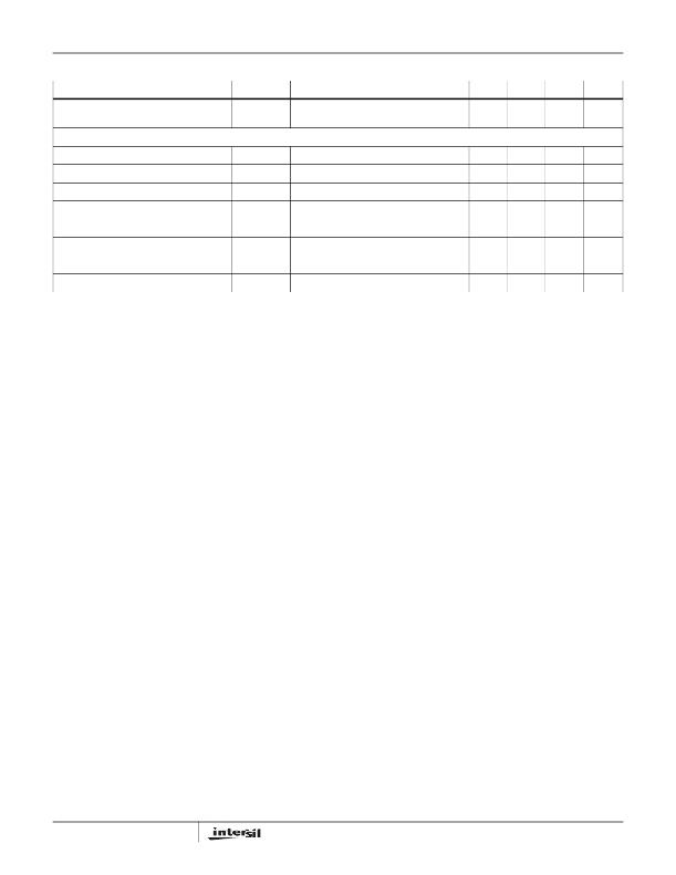
�Electrical� Specifications�
�Recommended� Operating� Conditions,� Unless� Otherwise� Noted.� (Continued)�
�PARAMETER�
�LGATE� Turn-On� Propagation� Delay�
�SYMBOL�
�t� PDHLGATE�
�TEST� CONDITIONS�
�V� VCC� =� 5V,� Outputs� Unloaded,�
�MIN�
�10�
�TYP�
�20�
�MAX�
�30�
�UNITS�
�ns�
�DELAY� =� VCC�
�OUTPUT�
�Upper� Drive� Source� Resistance�
�Upper� Driver� Source� Current� (Note� 5)�
�Upper� Drive� Sink� Resistance�
�Upper� Driver� Sink� Current� (Note� 5)�
�Lower� Drive� Source� Resistance�
�Lower� Driver� Source� Current� (Note� 5)�
�Lower� Drive� Sink� Resistance�
�Lower� Driver� Sink� Current� (Note� 5)�
�R� UGATE�
�I� UGATE�
�R� UGATE�
�I� UGATE�
�R� LGATE�
�I� LGATE�
�R� LGATE�
�I� LGATE�
�500mA� Source� Current�
�V� UGATE-PHASE� =� 2.5V�
�500mA� Sink� Current�
�V� UGATE-PHASE� =� 2.5V�
�500mA� Source� Current�
�V� LGATE� =� 2.5V�
�500mA� Sink� Current�
�V� LGATE� =� 2.5V�
�-�
�-�
�-�
�-�
�-�
�-�
�-�
�-�
�1.0�
�2.0�
�1.0�
�2.0�
�1.0�
�2.0�
�0.4�
�4.0�
�2.5�
�-�
�2.5�
�-�
�2.5�
�-�
�1.0�
�-�
�Ω�
�A�
�Ω�
�A�
�Ω�
�A�
�Ω�
�A�
�NOTE:�
�5.� Guaranteed� by� characterization,� not� 100%� tested� in� production.�
�Functional� Pin� Description�
�UGATE� (Pin� 1� for� SOIC-8,� Pin� 8� for� QFN)�
�The� UGATE� pin� is� the� upper� gate� drive� output.� Connect� to�
�the� gate� of� high-side� power� N-Channel� MOSFET.�
�BOOT� (Pin� 2� for� SOIC-8,� Pin� 1� for� QFN)�
�BOOT� is� the� floating� bootstrap� supply� pin� for� the� upper� gate�
�drive.� Connect� the� bootstrap� capacitor� between� this� pin� and�
�the� PHASE� pin.� The� bootstrap� capacitor� provides� the� charge�
�to� turn� on� the� upper� MOSFET.� See� the� Bootstrap� Diode� and�
�Capacitor� section� under� DESCRIPTION� for� guidance� in�
�choosing� the� appropriate� capacitor� value.�
�PWM� (Pin� 3� for� SOIC-8,� Pin� 2� for� QFN)�
�The� PWM� signal� is� the� control� input� for� the� driver.� The� PWM�
�signal� can� enter� three� distinct� states� during� operation,� see� the�
�three-state� PWM� Input� section� under� DESCRIPTION� for� further�
�details.� Connect� this� pin� to� the� PWM� output� of� the� controller.� In�
�addition,� place� a� 500k� Ω� resistor� to� ground� from� this� pin.� This�
�allows� for� proper� three-state� operation� under� all� start-up�
�conditions.�
�GND� (Pin� 4� for� SOIC-8,� Pin� 3� for� QFN)�
�GND� is� the� ground� pin.� All� signals� are� referenced� to� this�
�node.�
�LGATE� (Pin� 5� for� SOIC-8,� Pin� 4� for� QFN)�
�LGATE� is� the� lower� gate� drive� output.� Connect� to� gate� of� the�
�low-side� power� N-Channel� MOSFET.�
�VCC� (Pin� 6� for� SOIC-8,� Pin� 5� for� QFN)�
�Connect� the� VCC� pin� to� a� +5V� bias� supply.� Place� a� high�
�quality� bypass� capacitor� from� this� pin� to� GND.�
�DELAY� (Pin� 7� for� SOIC-8,� Pin� 6� for� QFN)�
�The� DELAY� pin� sets� the� dead-time� between� gate� switching�
�for� the� ISL6209.� Connect� a� resistor� to� GND� from� this� pin� to�
�adjust� the� dead-time,� refer� to� Figure� 4.� Tie� this� pin� to� VCC� to�
�disable� the� delay� circuitry.� See� Shoot-Through� Protection�
�section� for� more� detail.�
�PHASE� (Pin� 8� for� SOIC-8,� Pin� 7� for� QFN)�
�Connect� the� PHASE� pin� to� the� source� of� the� upper� MOSFET�
�and� the� drain� of� the� lower� MOSFET.� This� pin� provides� a�
�return� path� for� the� upper� gate� driver.�
�Description�
�Operation�
�Designed� for� speed,� the� ISL6209� dual� MOSFET� driver� controls�
�both� high-side� and� low-side� N-Channel� FETs� from� one�
�externally� provided� PWM� signal.�
�A� rising� edge� on� PWM� initiates� the� turn-off� of� the� lower�
�MOSFET� (see� Timing� Diagram).� After� a� short� propagation�
�delay� [t� PDLLGATE� ],� the� lower� gate� begins� to� fall.� Typical� fall�
�times� [t� FLGATE� ]� are� provided� in� the� Electrical� Specifications�
�section.� Adaptive� shoot-through� circuitry� monitors� the�
�LGATE� voltage� and� determines� the� upper� gate� delay� time�
�[t� PDHUGATE� ],� based� on� how� quickly� the� LGATE� voltage�
�drops� belo� w� 1V� .� This� prevents� both� the� lower� and� upper�
�MOSFETs� from� conducting� simultaneously,� or� shoot-�
�through.� Once� this� delay� period� is� completed,� the� upper� gate�
�drive� begins� to� rise� [t� RUGATE� ],� and� the� upper� MOSFET�
�turns� on.�
�A� falling� transition� on� PWM� indicates� the� turn-off� of� the� upper�
�MOSFET� and� the� turn-on� of� the� lower� MOSFET.� A� short�
�propagation� delay� [t� PDLUGATE� ]� is� encountered� before� the�
�upper� gate� begins� to� fall� [t� FUGATE� ].� Again,� the� adaptive�
�5�
�相关PDF资料 |
PDF描述 |
|---|---|
| 387-050-524-802 | CARDEDGE 50POS DL .156 PCB BLK |
| S1M-E3/61T | DIODE GPP 1A 1000V SMA |
| T95C106K025LSAS | CAP TANT 10UF 25V 10% 2812 |
| ISL6208CR-T | IC MOSFET DRVR SYNC BUCK 8-QFN |
| F721A227KRC | CAP TANT 220UF 10V 10% 2824 |
相关代理商/技术参数 |
参数描述 |
|---|---|
| ISL6209CB-T | 功能描述:IC MOSFET DRVR SYNC BUCK 8-SOIC RoHS:否 类别:集成电路 (IC) >> PMIC - MOSFET,电桥驱动器 - 外部开关 系列:- 标准包装:50 系列:- 配置:低端 输入类型:非反相 延迟时间:40ns 电流 - 峰:9A 配置数:1 输出数:1 高端电压 - 最大(自引导启动):- 电源电压:4.5 V ~ 35 V 工作温度:-40°C ~ 125°C 安装类型:表面贴装 封装/外壳:TO-263-6,D²Pak(5 引线+接片),TO-263BA 供应商设备封装:TO-263 包装:管件 |
| ISL6209CBZ | 功能描述:功率驱动器IC P6 HV SYNCHCT BUCK MSFT W/POR & DELAY RoHS:否 制造商:Micrel 产品:MOSFET Gate Drivers 类型:Low Cost High or Low Side MOSFET Driver 上升时间: 下降时间: 电源电压-最大:30 V 电源电压-最小:2.75 V 电源电流: 最大功率耗散: 最大工作温度:+ 85 C 安装风格:SMD/SMT 封装 / 箱体:SOIC-8 封装:Tube |
| ISL6209CBZ-T | 功能描述:功率驱动器IC P6 HV SYNCHCT BUCK MSFT W/POR & DELAY RoHS:否 制造商:Micrel 产品:MOSFET Gate Drivers 类型:Low Cost High or Low Side MOSFET Driver 上升时间: 下降时间: 电源电压-最大:30 V 电源电压-最小:2.75 V 电源电流: 最大功率耗散: 最大工作温度:+ 85 C 安装风格:SMD/SMT 封装 / 箱体:SOIC-8 封装:Tube |
| ISL6209CR | 制造商:Rochester Electronics LLC 功能描述:- Bulk |
| ISL6209CR-T | 制造商:INTERSIL 制造商全称:Intersil Corporation 功能描述:High Voltage Synchronous Rectified Buck MOSFET Driver |
发布紧急采购,3分钟左右您将得到回复。