- 您现在的位置:买卖IC网 > PDF目录20380 > ISL6209CB (Intersil)IC MOSFET DRVR SYNC BUCK 8-SOIC PDF资料下载
参数资料
| 型号: | ISL6209CB |
| 厂商: | Intersil |
| 文件页数: | 7/10页 |
| 文件大小: | 0K |
| 描述: | IC MOSFET DRVR SYNC BUCK 8-SOIC |
| 标准包装: | 98 |
| 配置: | 高端和低端,同步 |
| 输入类型: | PWM |
| 延迟时间: | 20ns |
| 电流 - 峰: | 2A |
| 配置数: | 1 |
| 输出数: | 2 |
| 高端电压 - 最大(自引导启动): | 33V |
| 电源电压: | 4.5 V ~ 5.5 V |
| 工作温度: | -10°C ~ 100°C |
| 安装类型: | 表面贴装 |
| 封装/外壳: | 8-SOIC(0.154",3.90mm 宽) |
| 供应商设备封装: | 8-SOIC |
| 包装: | 管件 |
�� �
�
�ISL6209�
�The� equation� governing� the� dead-time� seen� in� Figure� 4� is�
�expressed� as:�
�will� push� the� IC� beyond� the� maximum� recommended�
�operating� junction� temperature� of� 125°C.� The� maximum�
�T� DELAY� =� [� (� 160� � 10�
�–� 15�
�)� � R� DELAY� ]� +� 6ns�
�allowable� IC� power� dissipation� for� the� SO-8� package� is�
�approximately� 800mW.� When� designing� the� driver� into� an�
�application,� it� is� recommended� that� the� following� calculation�
�The� equation� can� be� rewritten� to� solve� for� R� DELAY� as�
�follows:�
�be� performed� to� ensure� safe� operation� at� the� desired�
�frequency� for� the� selected� MOSFETs.� The� power� dissipated�
�R� DELAY� =� --------------------------------------------�
�(� T� DELAY� –� 6ns� )�
�160� ×� 10� –� 15�
�by� the� driver� is� approximated� as:�
�P� =� f� sw� (� 1.5V� U� Q� U� +� V� L� Q� L� )� +� I� VCC� V�
�CC�
�Internal� Bootstrap� Diode�
�This� driver� features� an� internal� bootstrap� Schottky� diode.�
�Simply� adding� an� external� capacitor� across� the� BOOT� and�
�PHASE� pins� completes� the� bootstrap� circuit.�
�The� bootstrap� capacitor� must� have� a� maximum� voltage�
�rating� above� the� maximum� battery� voltage� plus� 5V.� The�
�where� f� sw� is� the� switching� frequency� of� the� PWM� signal.� V� U�
�and� V� L� represent� the� upper� and� lower� gate� rail� voltage.� Q� U�
�and� Q� L� is� the� upper� and� lower� gate� charge� determined� by�
�MOSFET� selection� and� any� external� capacitance� added� to�
�the� gate� pins.� The� I� VCC� V� CC� product� is� the� quiescent� power�
�of� the� driver� and� is� typically� negligible.�
�C� BOOT� ≥� ------------------------�
�bootstrap� capacitor� can� be� chosen� from� the� following�
�equation:�
�Q� GATE�
�Δ� V� BOOT�
�where� Q� GATE� is� the� amount� of� gate� charge� required� to� fully�
�charge� the� gate� of� the� upper� MOSFET.� The� Δ� V� BOOT� term� is�
�defined� as� the� allowable� droop� in� the� rail� of� the� upper� drive.�
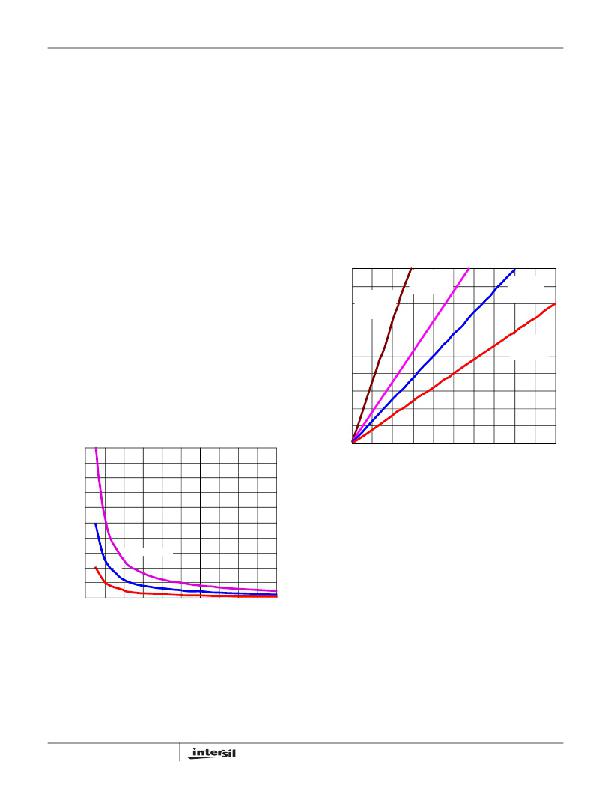
�1000�
�900�
�800�
�700�
�600�
�500�
�Q� U� =100nC�
�Q� L� =� 200nC�
�Q� U� =50nC�
�Q� L� =� 100nC�
�Q� U� =� 50nC�
�Q� L� =� 50nC�
�Q� U� =� 20nC�
�Q� L� =� 50nC�
�As� an� example,� suppose� an� upper� MOSFET� has� a� gate�
�charge,� Q� GATE� ,� of� 25nC� at� 5V� and� also� assume� the� droop� in�
�the� drive� voltage� over� a� PWM� cycle� is� 200mV.� One� will� find�
�that� a� bootstrap� capacitance� of� at� least� 0.125� μ� F� is� required.�
�The� next� larger� standard� value� capacitance� is� 0.22� μ� F.� A�
�good� quality� ceramic� capacitor� is� recommended.�
�400�
�300�
�200�
�100�
�2.0�
�0�
�0�
�200�
�400�
�600�
�800�
�1000� 1200� 1400� 1600� 1800� 2000�
�1.8�
�1.6�
�1.4�
�1.2�
�1.0�
�0.8�
�FREQUENCY� (kHz)�
�FIGURE� 6.� POWER� DISSIPATION� vs� FREQUENCY�
�Layout� Considerations�
�Reducing� Phase� Ring�
�The� parasitic� inductances� of� the� PCB� and� power� devices�
�0.6�
�0.4�
�Q� GATE� = 100nC�
�(both� upper� and� lower� FETs)� could� cause� increased� PHASE�
�ringing,� which� may� lead� to� voltages� that� exceed� the� absolute�
�20nC�
�0.2�
�0.0�
�0.0� 0.1�
�0.2�
�0.3�
�0.4� 0.5� 0.6�
�0.7�
�0.8�
�0.9�
�1.0�
�maximum� rating� of� the� devices.� When� PHASE� rings� below�
�ground,� the� negative� voltage� could� add� charge� to� the�
�bootstrap� capacitor� through� the� internal� bootstrap� diode.�
�Δ� V� BOOT_CAP� (V)�
�FIGURE� 5.� BOOTSTRAP� CAPACITANCE� vs� BOOT� RIPPLE�
�VOLTAGE�
�Power� Dissipation�
�Package� power� dissipation� is� mainly� a� function� of� the�
�switching� frequency� and� total� gate� charge� of� the� selected�
�MOSFETs.� Calculating� the� power� dissipation� in� the� driver� for�
�a� desired� application� is� critical� to� ensuring� safe� operation.�
�Exceeding� the� maximum� allowable� power� dissipation� level�
�7�
�Under� worst-case� conditions,� the� added� charge� could�
�overstress� the� BOOT� and/or� PHASE� pins.� To� prevent� this�
�from� happening,� the� user� should� perform� a� careful� layout�
�inspection� to� reduce� trace� inductances,� and� select� low� lead�
�inductance� MOSFETs� and� drivers.� D� 2� PAK� and� DPAK�
�packaged� MOSFETs� have� high� parasitic� lead� inductances,�
�as� opposed� to� SOIC-8.� If� higher� inductance� MOSFETs� must�
�be� used,� a� Schottky� diode� is� recommended� across� the� lower�
�MOSFET� to� clamp� negative� PHASE� ring.�
�相关PDF资料 |
PDF描述 |
|---|---|
| 387-050-524-802 | CARDEDGE 50POS DL .156 PCB BLK |
| S1M-E3/61T | DIODE GPP 1A 1000V SMA |
| T95C106K025LSAS | CAP TANT 10UF 25V 10% 2812 |
| ISL6208CR-T | IC MOSFET DRVR SYNC BUCK 8-QFN |
| F721A227KRC | CAP TANT 220UF 10V 10% 2824 |
相关代理商/技术参数 |
参数描述 |
|---|---|
| ISL6209CB-T | 功能描述:IC MOSFET DRVR SYNC BUCK 8-SOIC RoHS:否 类别:集成电路 (IC) >> PMIC - MOSFET,电桥驱动器 - 外部开关 系列:- 标准包装:50 系列:- 配置:低端 输入类型:非反相 延迟时间:40ns 电流 - 峰:9A 配置数:1 输出数:1 高端电压 - 最大(自引导启动):- 电源电压:4.5 V ~ 35 V 工作温度:-40°C ~ 125°C 安装类型:表面贴装 封装/外壳:TO-263-6,D²Pak(5 引线+接片),TO-263BA 供应商设备封装:TO-263 包装:管件 |
| ISL6209CBZ | 功能描述:功率驱动器IC P6 HV SYNCHCT BUCK MSFT W/POR & DELAY RoHS:否 制造商:Micrel 产品:MOSFET Gate Drivers 类型:Low Cost High or Low Side MOSFET Driver 上升时间: 下降时间: 电源电压-最大:30 V 电源电压-最小:2.75 V 电源电流: 最大功率耗散: 最大工作温度:+ 85 C 安装风格:SMD/SMT 封装 / 箱体:SOIC-8 封装:Tube |
| ISL6209CBZ-T | 功能描述:功率驱动器IC P6 HV SYNCHCT BUCK MSFT W/POR & DELAY RoHS:否 制造商:Micrel 产品:MOSFET Gate Drivers 类型:Low Cost High or Low Side MOSFET Driver 上升时间: 下降时间: 电源电压-最大:30 V 电源电压-最小:2.75 V 电源电流: 最大功率耗散: 最大工作温度:+ 85 C 安装风格:SMD/SMT 封装 / 箱体:SOIC-8 封装:Tube |
| ISL6209CR | 制造商:Rochester Electronics LLC 功能描述:- Bulk |
| ISL6209CR-T | 制造商:INTERSIL 制造商全称:Intersil Corporation 功能描述:High Voltage Synchronous Rectified Buck MOSFET Driver |
发布紧急采购,3分钟左右您将得到回复。