- 您现在的位置:买卖IC网 > PDF目录20543 > ISL6210CRZ-T (Intersil)IC MOSFET DRIVER DUAL SYNC 16QFN PDF资料下载
参数资料
| 型号: | ISL6210CRZ-T |
| 厂商: | Intersil |
| 文件页数: | 5/10页 |
| 文件大小: | 0K |
| 描述: | IC MOSFET DRIVER DUAL SYNC 16QFN |
| 标准包装: | 6,000 |
| 配置: | 高端和低端,同步 |
| 输入类型: | PWM |
| 延迟时间: | 26ns |
| 电流 - 峰: | 2A |
| 配置数: | 2 |
| 输出数: | 4 |
| 高端电压 - 最大(自引导启动): | 36V |
| 电源电压: | 4.5 V ~ 5.5 V |
| 工作温度: | -10°C ~ 100°C |
| 安装类型: | 表面贴装 |
| 封装/外壳: | 16-VQFN 裸露焊盘 |
| 供应商设备封装: | 16-QFN-EP(4x4) |
| 包装: | 带卷 (TR) |
�� �
�
�ISL6210�
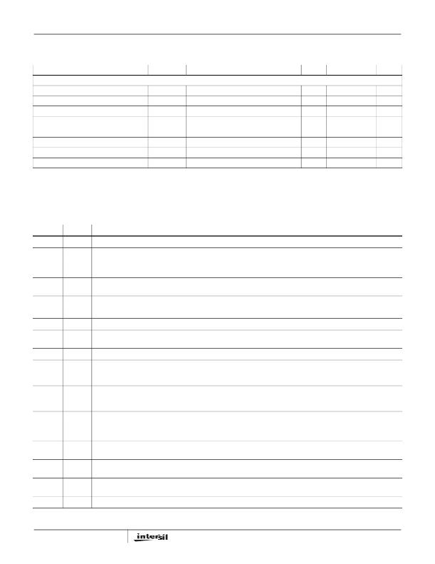
�Electrical� Specifications�
�These� specifications� apply� for� T� A� =� -10°C� to� +100°C,� Unless� Otherwise� Noted.� (Continued)� Parameters� with�
�MIN� and/or� MAX� limits� are� 100%� tested� at� +25°C,� unless� otherwise� specified.� Temperature� limits� established� by�
�characterization� and� are� not� production� tested.�
�PARAMETER�
�SYMBOL�
�TEST� CONDITIONS�
�MIN�
�TYP�
�MAX�
�UNITS�
�OUTPUT�
�Upper� Drive� Source� Resistance�
�Upper� Drive� Source� Current� (Note� 4)�
�Upper� Drive� Sink� Resistance�
�Upper� Drive� Sink� Current� (Note� 4)�
�Lower� Drive� Source� Resistance�
�Lower� Drive� Source� Current� (Note� 4)�
�Lower� Drive� Sink� Resistance�
�Lower� Drive� Sink� Current� (Note� 4)�
�R� UG_SRC�
�I� UG_SCR�
�R� UG_SNK�
�I� UG_SNK�
�R� LG_SRC�
�I� LG_SCR�
�R� LG_SNK�
�I� LG_SNK�
�250mA� Source� Current�
�V� UGATE-PHASE� =� 2.5V�
�250mA� Sink� Current�
�V� UGATE-PHASE� =� 2.5V�
�250mA� Source� Current�
�V� LGATE� =� 2.5V�
�250mA� Sink� Current�
�V� LGATE� =� 2.5V�
�-�
�-�
�-�
�-�
�-�
�-�
�-�
�1.0�
�2.00�
�1.0�
�2.00�
�1.0�
�2.00�
�0.4�
�4.00�
�2.5�
�-�
�2.5�
�-�
�2.5�
�-�
�1.0�
�-�
�Ω�
�A�
�Ω�
�A�
�Ω�
�A�
�Ω�
�A�
�NOTE:�
�3.� Parameters� with� MIN� and/or� MAX� limits� are� 100%� tested� at� +25°C,� unless� otherwise� specified.� Temperature� limits� established� by� characterization�
�and� are� not� production� tested.�
�4.� Limits� established� by� characterization� and� are� not� production� tested.�
�Functional� Pin� Description�
�NUMBER�
�1�
�2�
�3�
�4�
�5�
�6�
�7�
�NAME�
�GND�
�LGATE1�
�PVCC�
�FCCM�
�PGND�
�LGATE2�
�EN�
�FUNCTION�
�Bias� and� reference� ground.� All� signals� are� referenced� to� this� node.�
�Lower� gate� drive� output� of� Channel� 1.� Connect� to� gate� of� the� low-side� power� N-Channel� MOSFET.�
�This� pin� supplies� power� to� both� the� lower� and� higher� gate� drives� in� ISL6210.� Connect� to� a� +5V� supply.� Place� a� high� quality�
�low� ESR� ceramic� capacitor� from� this� pin� to� GND.�
�Logic� control� input� that� will� force� continuous� conduction� mode� (HIGH� state)� or� allow� discontinuous� conduction� mode�
�(LOW� state).� Placing� a� series� resistor� in� this� input� will� allow� the� switching� dead-time� to� be� programmed.�
�It� is� the� power� ground� return� of� both� low� gate� drivers.�
�Lower� gate� drive� output� of� Channel� 2.� Connect� to� gate� of� the� low-side� power� N-Channel� MOSFET.�
�Logic� control� input� that� will� enable� (HIGH� state)� or� disable� (LOW� state)� the� IC.� Shutdown� current� is� <1μA.�
�8�
�9�
�PHASE2� Connect� this� pin� to� the� SOURCE� of� the� upper� MOSFET� and� the� DRAIN� of� the� lower� MOSFET� in� Channel� 2.� This� pin�
�provides� a� return� path� for� the� upper� gate� drive.�
�UGATE2� Upper� gate� drive� output� of� Channel� 2.� Connect� to� gate� of� high-side� power� N-Channel� MOSFET.�
�10�
�11�
�BOOT2�
�BOOT1�
�Floating� bootstrap� supply� pin� for� the� upper� gate� drive� of� Channel� 2.� Connect� the� bootstrap� capacitor� between� this� pin� and�
�the� PHASE2� pin.� The� bootstrap� capacitor� provides� the� charge� to� turn� on� the� upper� MOSFET.� See� “Internal� Bootstrap� Diode”�
�on� page� 7� for� guidance� in� choosing� the� capacitor� value.�
�Floating� bootstrap� supply� pin� for� the� upper� gate� drive� of� Channel� 1.� Connect� the� bootstrap� capacitor� between� this� pin� and�
�the� PHASE1� pin.� The� bootstrap� capacitor� provides� the� charge� to� turn� on� the� upper� MOSFET.� See“Internal� Bootstrap� Diode”�
�on� page� 7� for� guidance� in� choosing� the� capacitor� value.�
�12�
�13�
�UGATE1� Upper� gate� drive� output� of� Channel� 1.� Connect� to� gate� of� high-side� power� N-Channel� MOSFET.�
�PHASE1� Connect� this� pin� to� the� SOURCE� of� the� upper� MOSFET� and� the� DRAIN� of� the� lower� MOSFET� in� Channel� 1.� This� pin�
�provides� a� return� path� for� the� upper� gate� drive.�
�14�
�15�
�16�
�N/A�
�VCC�
�PWM1�
�PWM2�
�PAD�
�Connect� a� +5V� bias� supply� to� this� pin.� It� supplies� the� internal� analog� circuits.� Place� a� high� quality,� low� ESR� ceramic� capacitor�
�from� this� pin� to� GND.� This� should� be� a� separate� capacitor� than� the� one� used� for� PVCC� (Pin� 3).�
�The� PWM� signal� is� the� control� input� for� the� Channel� 1� driver.� The� PWM� signal� can� enter� three� distinct� states� during� operation.� See�
�“Three-State� PWM� Input”� on� page� 6� for� further� details.� Connect� this� pin� to� the� PWM� output� of� the� controller.�
�The� PWM� signal� is� the� control� input� for� the� Channel� 2� driver.� The� PWM� signal� can� enter� three� distinct� states� during� operation.� See�
�“Three-State� PWM� Input”� on� page� 6� for� further� details.� Connect� this� pin� to� the� PWM� output� of� the� controller.�
�Connect� this� pad� to� the� power� ground� plane� (GND)� via� thermally� enhanced� connection.�
�5�
�FN6392.1�
�December� 9,� 2008�
�相关PDF资料 |
PDF描述 |
|---|---|
| T525T336M010ATE080 | CAP TANT 33UF 10V 20% 1411 |
| GBC19DRXH | CONN EDGECARD 38POS DIP .100 SLD |
| A7OOB-1506M | CABLE D-SUB-AFN15B/AE15M/AFN15B |
| RCD-24-0.50/W/X1 | LED SUPPLY CC BUCK 2-35V 0.5A |
| VI-BN4-CY-B1 | CONVERTER MOD DC/DC 48V 50W |
相关代理商/技术参数 |
参数描述 |
|---|---|
| ISL6211 | 制造商:INTERSIL 制造商全称:Intersil Corporation 功能描述:Crusoe⑩ Processor Core-Voltage Regulator |
| ISL6211CA | 制造商:Rochester Electronics LLC 功能描述:CPU REGULATOR FOR TRANSMETA,SINGLE CORE - Bulk 制造商:Intersil Corporation 功能描述: |
| ISL6211CA WAF | 制造商:Intersil Corporation 功能描述: |
| ISL6211CA-T | 制造商:Rochester Electronics LLC 功能描述:CPU REGULATOR FOR TRANSMETA,SINGLE CORE - Tape and Reel 制造商:Intersil Corporation 功能描述: |
| ISL6215CA | 制造商:Rochester Electronics LLC 功能描述:C4AM,PRECISION MULTI-PHASE BUCK PWM CONT - Bulk |
发布紧急采购,3分钟左右您将得到回复。