- 您现在的位置:买卖IC网 > PDF目录16600 > ISL6218CVZA (Intersil)IC CTRLR INTEL PENT M 38-TSSOP PDF资料下载
参数资料
| 型号: | ISL6218CVZA |
| 厂商: | Intersil |
| 文件页数: | 12/19页 |
| 文件大小: | 0K |
| 描述: | IC CTRLR INTEL PENT M 38-TSSOP |
| 标准包装: | 50 |
| 应用: | 处理器 |
| 电流 - 电源: | 1.4mA |
| 电源电压: | 4.75 V ~ 5.25 V |
| 工作温度: | -10°C ~ 85°C |
| 安装类型: | 表面贴装 |
| 封装/外壳: | 38-TFSOP(0.173",4.40mm 宽) |
| 供应商设备封装: | 38-TSSOP |
| 包装: | 管件 |
�� �
�
�ISL6218�
�shutting� off� the� low� side� MOSFET.� This� “Three-State”� mode�
�will� hold� both� upper� and� low� side� MOSFETs� off� during� the�
�BATTERY�
�time� that� the� Low� Side� MOSFET� would� normally� be� on.�
�This� “Diode� Emulation”� is� initiated� when� the� current,� as�
�sensed� through� the� low� side� MOSFET,� is� negative.� This� event�
�V� REF� =� 1.75V�
�I� OCSET�
�ISL6218�
�OCSET�
�triggers� the� “Three-State”� mode� until� the� next� PWM� cycle.�
�R1�
�36.5k�
�VBAT�
�This� Discontinuous� operation� improves� efficiency� by� preventing�
�the� reverse� conduction� of� current� through� the� low� side�
�MOSFET.� This� eliminates� conduction� loss� and� output�
�discharge.� Discontinuous� operation� is� enabled� in� Deep� and�
�Deeper� Sleep� modes� and� is� based� solely� on� current� feedback.�
�R2�
�1.200V�
�30.1k�
�0.750V�
�STV�
�DRSV�
�DACOUT�
�VID� COMMAND�
�VOLTAGE�
�1.21k�
�Due� to� this� ISL6218’s� ability� to� sense� zero� current� and�
�prevent� discharging� through� the� low� side� MOSFETs� during�
�R3�
�49.9k�
�SOFT�
�GND�
�DSV�
�98.8%�
�DACOUT�
�light� loads,� the� ISL6218� meets� the� requirements� for� PSI�
�without� requiring� any� external� signals.�
�STV,� DSV� and� DRSV�
�0.012μF�
�98.8k�
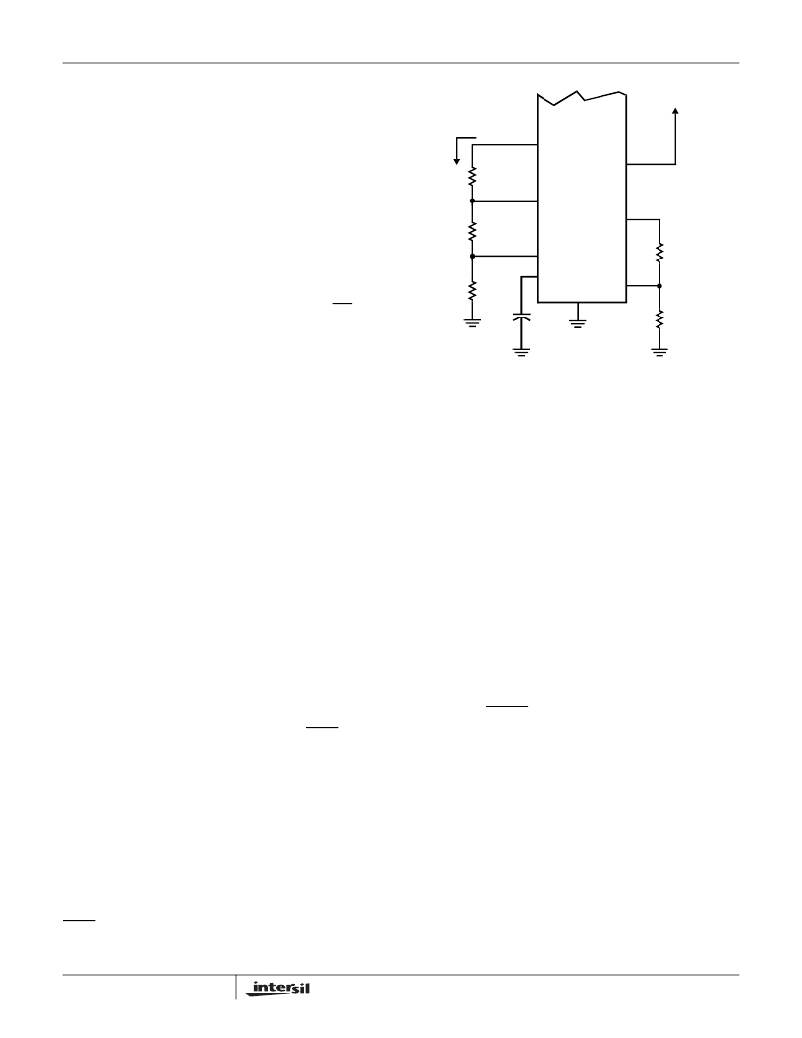
�START-UP� “BOOT”� VOLTAGE� -� STV�
�The� Start-up,� or� “Boot,”� voltage� is� programmed� by� an�
�external� resistor� divider� network� from� the� OCSET� pin� (refer�
�to� Figure� 8).� Internally,� a� 1.75V� reference� voltage� is� output�
�on� the� OCSET� pin.� The� start-up� voltage� is� set� through� a�
�voltage� divider� from� the� 1.75V� reference� at� the� OCSET� pin.�
�The� voltage� on� the� STV� pin� will� be� the� controller� regulating�
�voltage� during� the� start-up� sequence.�
�Once� the� PGOOD� pin� of� the� ISL6218� controller� is� externally�
�enabled� high� by� the� Vccp� and� Vcc_mch� controllers,� the�
�ISL6218� will� then� ramp,� after� a� 10μs� delay,� to� the� voltage�
�commanded� by� the� VID� setting� minus� “Droop”.�
�DEEP� SLEEP� VOLTAGE-� DSV�
�The� Deep� Sleep� voltage� is� programmed� by� an� external�
�voltage� divider� network� from� the� DACOUT� pin� (Refer� to�
�Figure� 8).� The� DACOUT� pin� is� the� output� of� the� VID� digital-�
�to-analog� converter.� By� having� the� Deep� Sleep� voltage� setup�
�from� a� resistor� divider� from� DAC,� the� Deep� Sleep� voltage� will�
�be� a� constant� percentage� of� the� VID.� Through� the� voltage�
�FIGURE� 8.� CONFIGURATIONS� FOR� BATTERY� INPUT,�
�OVERCURRENT� SETTING� AND� START,� DEEP�
�SLEEP� AND� DEEPER� SLEEP� VOLTAGE�
�OVERCURRENT� SETTING� -� OCSET�
�The� ISL6218� overcurrent� protection� essentially� compares� a�
�user-selectable� overcurrent� threshold� to� the� scaled� and�
�sampled� output� current.� An� overcurrent� condition� is� defined�
�when� the� sampled� current� is� equal� to� or� greater� than� the�
�threshold� current.� A� step� by� step� process� to� the� user-desired�
�overcurrent� set� point� is� detailed� next.�
�Step� 1:� Setting� the� Overcurrent� Threshold�
�The� overcurrent� threshold� is� represented� by� the� DC� current�
�flowing� out� of� the� OCSET� pin� (See� Figure� 8).� Since� the�
�OCSET� pin� is� held� at� a� constant� 1.75V,� the� user� need� only�
�populate� a� resistor� from� this� pin� to� ground� to� set� the� desired�
�overcurrent� threshold,� I� OCSET� .� The� user� should� pick� a� value�
�of� I� OCSET� between� 10μA� and� 15μA.� Once� this� is� done,� use�
�Ohm’s� Law� to� determine� the� necessary� resistor� to� place� from�
�OCSET� to� ground:�
�divider� network,� Deep� Sleep� voltage� is� set� to� 98.8%� of� the�
�programmed� VID� voltage,� as� per� the� IMVP-IV� ?� specification.�
�R� OCSET� =�
�1� .� 75� V�
�I� OCSET�
�=� R� 1� +� R� 2� +� R� 3�
�(EQ.� 2)�
�The� IC� enters� the� Deep� Sleep� mode� when� the� DSEN� is� low�
�and� the� DRSEN� pin� is� low� as� shown� in� Figure� 6� and�
�Figure� 5.� Once� in� Deep� Sleep� Mode,� the� controller� will�
�regulate� to� the� voltage� seen� on� the� DSV� pin� minus� “Droop”.�
�DEEPER� SLEEP� VOLTAGE� -� DRSV�
�The� Deeper� Sleep� voltage,� DRSV,� is� programmed� by� an�
�external� voltage� divider� network� from� the� 1.75V� reference� on�
�the� OCSET� pin� (Refer� to� Figure� 8).� In� Deeper� Sleep� mode�
�the� ISL6218� controller� will� regulate� the� output� voltage� to� the�
�voltage� present� on� the� DRSV� pin� minus� “Droop”.�
�The I� C� enters� Deeper� Sleep� mode� when� DRSEN� is� high� and�
�DSEN� is� low,� as� shown� in� Figure� 5.�
�12�
�For� example,� if� the� desired� overcurrent� threshold� is� 15μA,�
�the� total� resistance� from� OCSET� must� equal� 117k� Ω� .�
�Step� 2:� Selecting� ISEN� Resistance� for� Desired�
�Overcurrent� Level�
�After� choosing� the� I� OCSET� level,� the� user� must� then� decide�
�what� level� of� total� output� current� is� desired� for� overcurrent.�
�Typically,� this� number� is� between� 150%� and� 200%� of� the�
�maximum� operating� current� of� the� application.� For� example,�
�if� the� max� operating� current� is� 27A,� and� the� user� chooses�
�150%� overcurrent,� the� ISL6218� will� shut� down� if� the� output�
�current� exceeds� 27A*1.5� or� 40A.� According� to� the� “Block�
��determine� R� ISEN� once� the� overcurrent� level,� I� OC� ,� is� chosen.�
�FN9101.6�
�August� 6,� 2007�
�相关PDF资料 |
PDF描述 |
|---|---|
| VE-BNH-EW | CONVERTER MOD DC/DC 52V 100W |
| GEM18DSEF | CONN EDGECARD 36POS .156 EYELET |
| EET-ED2D391BA | CAP ALUM 390UF 200V 20% SNAP |
| 6-837975-4 | LGH MLD END ELECT LEAD |
| EET-UQ2D471BA | CAP ALUM 470UF 200V 20% SNAP |
相关代理商/技术参数 |
参数描述 |
|---|---|
| ISL6218CVZA-T | 功能描述:电流型 PWM 控制器 W/ANNEAL P6 MULTIPHS BUCK PWM CONTR RoHS:否 制造商:Texas Instruments 开关频率:27 KHz 上升时间: 下降时间: 工作电源电压:6 V to 15 V 工作电源电流:1.5 mA 输出端数量:1 最大工作温度:+ 105 C 安装风格:SMD/SMT 封装 / 箱体:TSSOP-14 |
| ISL6218CVZ-T | 功能描述:电流型 PWM 控制器 P6 MULTIPHS BUCK PWM CNTRLR FOR IMVP4 RoHS:否 制造商:Texas Instruments 开关频率:27 KHz 上升时间: 下降时间: 工作电源电压:6 V to 15 V 工作电源电流:1.5 mA 输出端数量:1 最大工作温度:+ 105 C 安装风格:SMD/SMT 封装 / 箱体:TSSOP-14 |
| ISL6218EVAL2 | 功能描述:EVALUATION BOARD 2 FOR ISL6218 RoHS:否 类别:编程器,开发系统 >> 评估板 - DC/DC 与 AC/DC(离线)SMPS 系列:- 产品培训模块:Obsolescence Mitigation Program 标准包装:1 系列:True Shutdown™ 主要目的:DC/DC,步升 输出及类型:1,非隔离 功率 - 输出:- 输出电压:- 电流 - 输出:1A 输入电压:2.5 V ~ 5.5 V 稳压器拓扑结构:升压 频率 - 开关:3MHz 板类型:完全填充 已供物品:板 已用 IC / 零件:MAX8969 |
| ISL6219 | 制造商:INTERSIL 制造商全称:Intersil Corporation 功能描述:Microprocessor CORE Voltage Regulator Precision Multi-Phase BUCK PWM Controller for Mobile Applications |
| ISL6219 WAF | 制造商:Harris Corporation 功能描述: |
发布紧急采购,3分钟左右您将得到回复。