- 您现在的位置:买卖IC网 > PDF目录16719 > ISL62391HRTZ-T (Intersil)IC PWR SUPPLY CONTROLLER 28TQFN PDF资料下载
参数资料
| 型号: | ISL62391HRTZ-T |
| 厂商: | Intersil |
| 文件页数: | 18/21页 |
| 文件大小: | 0K |
| 描述: | IC PWR SUPPLY CONTROLLER 28TQFN |
| 标准包装: | 6,000 |
| 应用: | 电源控制器 |
| 电源电压: | 5.5 V ~ 25 V |
| 电流 - 电源: | 150µA |
| 工作温度: | -10°C ~ 100°C |
| 安装类型: | 表面贴装 |
| 封装/外壳: | 28-WFQFN 裸露焊盘 |
| 供应商设备封装: | 28-TQFN-EP(4x4) |
| 包装: | 带卷 (TR) |
�� �
�
�ISL62391,� ISL62392,� ISL62391C,� ISL62392C�
�The� inductance� of� the� capacitor� can� cause� a� brief� voltage� dip�
�if� the� load� transient� has� an� extremely� high� slew� rate.� Low�
�inductance� capacitors� should� be� considered� in� this� scenario.�
�A� capacitor� dissipates� heat� as� a� function� of� RMS� current� and�
�frequency.� Be� sure� that� I� P-P� is� shared� by� a� sufficient� quantity�
�of� paralleled� capacitors� so� that� they� operate� below� the�
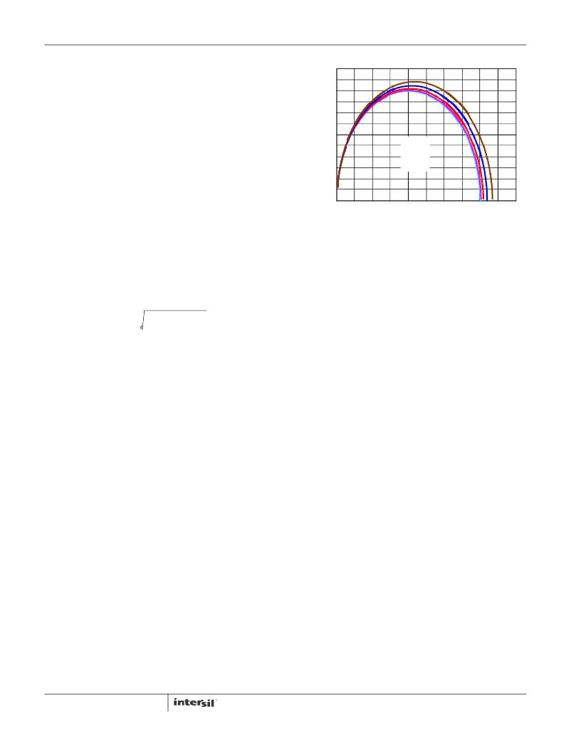
�0.60�
�0.55�
�0.50�
�0.45�
�0.40�
�maximum� rated� RMS� current� at� f� SW� .� Take� into� account� that�
�the� rated� value� of� a� capacitor� can� fade� as� much� as� 50%� as�
�the� DC� voltage� across� it� increases.�
�Selection� of� the� Input� Capacitor�
�The� important� parameters� for� the� bulk� input� capacitance� are�
�the� voltage� rating� and� the� RMS� current� rating.� For� reliable�
�0.35�
�0.30�
�0.25�
�0.20�
�0.15�
�0.10�
�0.05�
�x=1�
�x� =� 0.75�
�x� =� 0.50�
�x� =� 0.25�
�x=0�
�operation,� select� bulk� capacitors� with� voltage� and� current�
�ratings� above� the� maximum� input� voltage� and� capable� of�
�supplying� the� RMS� current� required� by� the� switching� circuit.�
�Their� voltage� rating� should� be� at� least� 1.25x� greater� than� the�
�0�
�0� 0.1� 0.2� 0.3� 0.4� 0.5� 0.6� 0.7� 0.8� 0.9�
�DUTY� CYCLE�
�FIGURE� 28.� NORMALIZED� RMS� INPUT� CURRENT�
�1.0�
�maximum� input� voltage,� while� a� voltage� rating� of� 1.5x� is� a�
�preferred� rating.� Figure� 28� is� a� graph� of� the� input� RMS� ripple�
�current� (normalized� relative� to� output� load� current)� as� a�
�function� of� duty� cycle� and� is� adjusted� for� a� converter� efficiency�
�of� 80%.� The� ripple� current� calculation� is� written� as�
�Equation� 21:�
�MOSFET� Selection� and� Considerations�
�Typically,� a� MOSFET� cannot� tolerate� even� brief� excursions�
�beyond� their� maximum� drain� to� source� voltage� rating.� The�
�MOSFETs� used� in� the� power� stage� of� the� converter� should�
�have� a� maximum� V� DS� rating� that� exceeds� the� sum� of� the�
�upper� voltage� tolerance� of� the� input� power� source� and� the�
�(� D� –� D� )� +� ?� D� ?� ------� ?�
�I� IN_RMS� ,� NORMALIZED� =�
�?� 12� ?�
�2� x�
�2�
�(EQ.� 21)�
�voltage� spike� that� occurs� when� the� MOSFET� switches� off.�
�There� are� several� power� MOSFETs� readily� available� that� are�
�Where:�
�-� I� MAX� is� the� maximum� continuous� I� LOAD� of� the� converter�
�-� x� is� a� multiplier� (0� to� 1)� corresponding� to� the� inductor�
�peak-to-peak� ripple� amplitude� expressed� as� a�
�percentage� of� I� MAX� (0%� to� 100%)�
�-� D� is� the� duty� cycle� that� is� adjusted� to� take� into� account�
�the� efficiency� of� the� converter� which� is� written� as�
�Equation� 22.�
�optimized� for� DC/DC� converter� applications.� The� preferred�
�high-side� MOSFET� emphasizes� low� gate� charge� so� that� the�
�device� spends� the� least� amount� of� time� dissipating� power� in�
�the� linear� region.� Unlike� the� low-side� MOSFET,� which� has�
�the� drain-source� voltage� clamped� by� its� body� diode� during�
�turn� off,� the� high-side� MOSFET� turns� off� with� a� V� DS� of�
�approximately� V� IN� -� V� OUT� ,� plus� the� spike� across� it.� The�
�preferred� low-side� MOSFET� emphasizes� low� r� DS(ON)� when�
�fully� saturated� to� minimize� conduction� loss.� It� should� be�
�V� O�
�V� IN� ?� EFF�
�D� =� --------------------------�
�(EQ.� 22)�
�noted� that� this� is� an� optimal� configuration� of� MOSFET�
�selection� for� low� duty� cycle� applications� (D� <� 50%).� For�
�In� addition� to� the� bulk� capacitance,� some� low� ESL� ceramic�
�capacitance� is� recommended� to� decouple� between� the� drain�
�of� the� high-side� MOSFET� and� the� source� of� the� low-side�
�MOSFET.�
�higher� output,� low� input� voltage� solutions,� a� more� balanced�
�MOSFET� selection� for� high-� and� low-side� devices� may� be�
�warranted.�
�For� the� low-side� (LS)� MOSFET,� the� power� loss� can� be�
�assumed� to� be� conductive� only� and� is� written� as� Equation� 23:�
�P� CON_LS� ≈� I� LOAD� ?� r� DS� (� ON� )� _LS� ?� (� 1� –� D� )�
�2�
�(EQ.� 23)�
�For� the� high-side� (HS)� MOSFET,� the� conduction� loss� is�
�written� as� Equation� 24:�
�P� CON_HS� =� I� LOAD�
�2�
�?�
�r� DS� (� ON� )� _HS� ?� D�
�(EQ.� 24)�
�P� SW_HS� =� -----------------------------------------------------------------� +� -------------------------------------------------------------�
�For� the� high-side� MOSFET,� the� switching� loss� is� written� as�
�Equation� 25:�
�V� IN� ?� I� VALLEY� ?� t� ON� ?� f� SW� V� IN� ?� I� PEAK� ?� t� OFF� ?� f� SW�
�2� 2�
�(EQ.� 25)�
�18�
�FN6666.7�
�August� 22,� 2013�
�相关PDF资料 |
PDF描述 |
|---|---|
| GEA28DTMH | CONN EDGECARD 56POS R/A .125 SLD |
| RCC05DRYN-S93 | CONN EDGECARD 10POS DIP .100 SLD |
| V375C15E150B | CONVERTER MOD DC/DC 15V 150W |
| ECM22DTBH | CONN EDGECARD 44POS R/A .156 SLD |
| ISL6126IRZA-T | IC POWER SUPPLY SEQUENCER 24QFN |
相关代理商/技术参数 |
参数描述 |
|---|---|
| ISL62391IRTZ | 功能描述:IC PWR SUPPLY CONTROLLER 28TQFN RoHS:是 类别:集成电路 (IC) >> PMIC - 电源控制器,监视器 系列:- 产品培训模块:Lead (SnPb) Finish for COTS Obsolescence Mitigation Program 标准包装:2,500 系列:- 应用:多相控制器 输入电压:- 电源电压:9 V ~ 14 V 电流 - 电源:- 工作温度:-40°C ~ 85°C 安装类型:表面贴装 封装/外壳:40-WFQFN 裸露焊盘 供应商设备封装:40-TQFN-EP(5x5) 包装:带卷 (TR) |
| ISL62391IRTZ-T | 功能描述:IC PWR SUPPLY CONTROLLER 28TQFN RoHS:是 类别:集成电路 (IC) >> PMIC - 电源控制器,监视器 系列:- 产品培训模块:Lead (SnPb) Finish for COTS Obsolescence Mitigation Program 标准包装:2,500 系列:- 应用:多相控制器 输入电压:- 电源电压:9 V ~ 14 V 电流 - 电源:- 工作温度:-40°C ~ 85°C 安装类型:表面贴装 封装/外壳:40-WFQFN 裸露焊盘 供应商设备封装:40-TQFN-EP(5x5) 包装:带卷 (TR) |
| ISL62391LOEVAL1Z | 功能描述:EVALUATION BOARD FOR ISL62391LO RoHS:是 类别:编程器,开发系统 >> 评估板 - DC/DC 与 AC/DC(离线)SMPS 系列:Robust Ripple Regulator™ (R³) 产品培训模块:Obsolescence Mitigation Program 标准包装:1 系列:True Shutdown™ 主要目的:DC/DC,步升 输出及类型:1,非隔离 功率 - 输出:- 输出电压:- 电流 - 输出:1A 输入电压:2.5 V ~ 5.5 V 稳压器拓扑结构:升压 频率 - 开关:3MHz 板类型:完全填充 已供物品:板 已用 IC / 零件:MAX8969 |
| ISL62392CHRTZ | 功能描述:IC PWR SUPPLY CTRLR 28TQFN RoHS:是 类别:集成电路 (IC) >> PMIC - 电源控制器,监视器 系列:- 产品培训模块:Lead (SnPb) Finish for COTS Obsolescence Mitigation Program 标准包装:2,500 系列:- 应用:多相控制器 输入电压:- 电源电压:9 V ~ 14 V 电流 - 电源:- 工作温度:-40°C ~ 85°C 安装类型:表面贴装 封装/外壳:40-WFQFN 裸露焊盘 供应商设备封装:40-TQFN-EP(5x5) 包装:带卷 (TR) |
| ISL62392CHRTZ-T | 功能描述:IC PWR SUPPLY CTRLR 28TQFN RoHS:是 类别:集成电路 (IC) >> PMIC - 电源控制器,监视器 系列:- 产品培训模块:Lead (SnPb) Finish for COTS Obsolescence Mitigation Program 标准包装:2,500 系列:- 应用:多相控制器 输入电压:- 电源电压:9 V ~ 14 V 电流 - 电源:- 工作温度:-40°C ~ 85°C 安装类型:表面贴装 封装/外壳:40-WFQFN 裸露焊盘 供应商设备封装:40-TQFN-EP(5x5) 包装:带卷 (TR) |
发布紧急采购,3分钟左右您将得到回复。