参数资料
| 型号: | ISL62883HRTZ-T |
| 厂商: | Intersil |
| 文件页数: | 15/37页 |
| 文件大小: | 0K |
| 描述: | IC REG PWM 3PHASE BUCK 40TQFN |
| 标准包装: | 6,000 |
| 应用: | 控制器,Intel IMVP-6.5? |
| 输入电压: | 5 V ~ 21 V |
| 输出数: | 1 |
| 输出电压: | 0.013 V ~ 1.5 V |
| 工作温度: | -10°C ~ 100°C |
| 安装类型: | 表面贴装 |
| 封装/外壳: | 40-WFQFN 裸露焊盘 |
| 供应商设备封装: | 40-TQFN-EP(5x5) |
| 包装: | 带卷 (TR) |
第1页第2页第3页第4页第5页第6页第7页第8页第9页第10页第11页第12页第13页第14页当前第15页第16页第17页第18页第19页第20页第21页第22页第23页第24页第25页第26页第27页第28页第29页第30页第31页第32页第33页第34页第35页第36页第37页
�� �
�
�ISL62883,� ISL62883B�
�VCC� SENSE� +� V� =� V� DAC� +� VSS� SENSE�
�Differential� Sensing�
�Figure� 9� also� shows� the� differential� voltage� sensing� scheme.�
�VCC� SENSE� and� VSS� SENSE� are� the� remote� voltage� sensing� signals�
�from� the� processor� die.� A� unity� gain� differential� amplifier� senses� the�
�VSS� SENSE� voltage� and� add� it� to� the� DAC� output.� The� error� amplifier�
�regulates� the� inverting� and� the� non-inverting� input� voltages� to� be�
�equal� as� shown� in� Equation� 3:�
�(EQ.� 3)�
�droop�
�The� ISL62883� will� adjust� the� phase� pulse-width� relative� to� the�
�other� phases� to� make� V� ISEN1� =� V� ISEN2� =� V� ISEN3� ,� thus� to� achieve�
�I� L1� =� I� L2� =� I� L3� ,� when� there� are� R� dcr1� =� R� dcr2� =� R� dcr3� and�
�R� pcb1� =� R� pcb2� =� R� pcb3� .�
�Using� same� components� for� L1,� L2� and� L3� will� provide� a� good�
�match� of� R� dcr1� ,� R� dcr2� and� R� dcr3� .� Board� layout� will� determine�
�R� pcb1� ,� R� pcb2� and� R� pcb3� .� It� is� recommended� to� have� symmetrical�
�layout� for� the� power� delivery� path� between� each� inductor� and� the�
�output� voltage� rail,� such� that� R� pcb1� =� R� pcb2� =� R� pcb3� .�
�Rpcb3�
�V3n�
�V2n�
�Rpcb1�
�V1n�
�Rewriting� Equation� 3� and� substitution� of� Equation� 2� gives:�
�VCC� SENSE� –� VSS� SENSE� =� V� DAC� –� R� droop� ×� I� droop� (EQ.� 4)�
�Equation� 4� is� the� exact� equation� required� for� load� line�
�implementation.�
�The� VCC� SENSE� and� VSS� SENSE� signals� come� from� the� processor�
�die.� The� feedback� will� be� open� circuit� in� the� absence� of� the�
�processor.� As� shown� in� Figure� 9,� it� is� recommended� to� add� a�
�“catch”� resistor� to� feed� the� VR� local� output� voltage� back� to� the�
�compensator,� and� add� another� “catch”� resistor� to� connect� the� VR�
�local� output� ground� to� the� RTN� pin.� These� resistors,� typically�
�10� Ω� ~100� Ω� ,� will� provide� voltage� feedback� if� the� system� is�
�powered� up� without� a� processor� installed.�
�ISEN3�
�INTERNAL�
�TO� IC�
�ISEN2�
�ISEN1�
�V3p�
�Phase3�
�Rs�
�Rs�
�Cs�
�Rs�
�V2p�
�Phase2�
�Rs�
�Rs�
�Cs�
�Rs�
�V1p�
�Phase1�
�Rs�
�Rs�
�Cs�
�L3�
�L2�
�L1�
�Rdcr3�
�IL3�
�Rdcr2� Rpcb2�
�IL2�
�Rdcr1�
�IL1�
�Vo�
�Phase� Current� Balancing�
�Rs�
�ISEN3�
�Phase3�
�Rs�
�L3�
�IL3�
�Rdcr3�
�Rpcb3�
�FIGURE� 11.� DIFFERENTIAL-SENSING� CURRENT� BALANCING�
�CIRCUIT�
�INTERNAL�
�TO� IC�
�ISEN2�
�ISEN1�
�Cs�
�Phase2�
�Rs�
�Cs�
�Phase1�
�Rs�
�Cs�
�L2�
�L1�
�IL2�
�IL1�
�Rdcr2�
�Rdcr1�
�Rpcb2�
�Rpcb1�
�Vo�
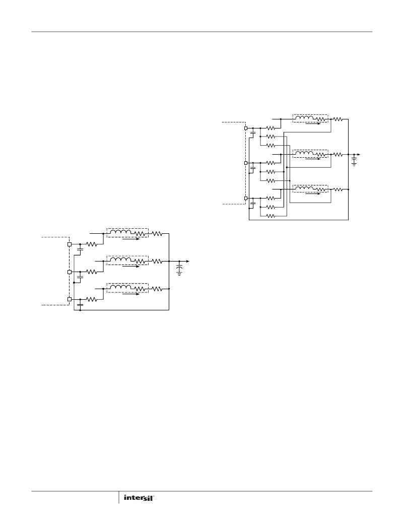
�Sometimes,� it� is� difficult� to� implement� symmetrical� layout.� For�
�the� circuit� shown� in� Figure� 10,� asymmetric� layout� causes�
�different� R� pcb1� ,� R� pcb2� and� R� pcb3� thus� current� imbalance.�
�Figure� 11� shows� a� differential-sensing� current� balancing� circuit�
�recommended� for� ISL62883.� The� current� sensing� traces� should�
�be� routed� to� the� inductor� pads� so� they� only� pick� up� the� inductor�
�DCR� voltage.� Each� ISEN� pin� sees� the� average� voltage� of� three�
�sources:� its� own� phase� inductor� phase-node� pad,� and� the� other�
�two� phases� inductor� output� side� pads.� Equations� 8� thru� 10� give�
�FIGURE� 10.� CURRENT� BALANCING� CIRCUIT�
�The� ISL62883� monitors� individual� phase� average� current� by�
�monitoring� the� ISEN1,� ISEN2,� and� ISEN3� voltages.� Figure� 10�
�shows� the� current� balancing� circuit� recommended� for� ISL62883.�
�Each� phase� node� voltage� is� averaged� by� a� low-pass� filter�
�the� ISEN� pin� voltages:�
�V� ISEN1� =� V� 1p� +� V� 2n� +� V� 3n�
�V� ISEN2� =� V� 1n� +� V� 2p� +� V� 3n�
�V� ISEN3� =� V� 1n� +� V� 2n� +� V� 3p�
�(EQ.� 8)�
�(EQ.� 9)�
�(EQ.� 10)�
�consisting� of� R� s� and� C� s� ,� and� presented� to� the� corresponding� ISEN�
�pin.� R� s� should� be� routed� to� inductor� phase-node� pad� in� order� to�
�eliminate� the� effect� of� phase� node� parasitic� PCB� DCR.�
�The� ISL62883� will� make� V� ISEN1� =� V� ISEN2� =� V� ISEN3� as� in:�
�V� 1p� +� V� 2n� +� V� 3n� =� V� 1n� +� V� 2p� +� V� 3n� (EQ.� 11)�
�Equations� 5� thru� 7� give� the� ISEN� pin� voltages:�
�V� 1n� +� V� 2p� +� V� 3n� =� V� 1n� +� V� 2n� +� V� 3p�
�(EQ.� 12)�
�V� ISEN1� =� (� R� dcr1� +� R� pcb1� )� � I� L1�
�(EQ.� 5)�
�Rewriting� Equation� 11� gives:�
�V� ISEN2� =� (� R� dcr2� +� R� pcb2� )� � I� L2�
�V� ISEN3� =� (� R� dcr3� +� R� pcb3� )� � I� L3�
�(EQ.� 6)�
�(EQ.� 7)�
�V� 1p� –� V� 1n� =� V� 2p� –� V� 2n�
�and� rewriting� Equation� 12� gives:�
�V� 2p� –� V� 2n� =� V� 3p� –� V� 3n�
�(EQ.� 13)�
�(EQ.� 14)�
�where� R� dcr1� ,� R� dcr2� and� R� dcr3� are� inductor� DCR;� R� pcb1� ,� R� pcb2�
�and� R� pcb3� are� parasitic� PCB� DCR� between� the� inductor� output�
�side� pad� and� the� output� voltage� rail;� and� I� L1� ,� I� L2� and� I� L3� are�
�inductor� average� currents.�
�15�
�Combining� Equations� 13� and� 14� gives� :�
�V� 1p� –� V� 1n� =� V� 2p� –� V� 2n� =� V� 3p� –� V� 3n�
�Therefore:�
�R� dcr1� � I� L1� =� R� dcr2� � I� L2� =� R� dcr3� � I� L3�
�(EQ.� 15)�
�(EQ.� 16)�
�FN6891.4�
�June� 21,� 2011�
�相关PDF资料 |
PDF描述 |
|---|---|
| RCM22DTBD-S189 | CONN EDGECARD 44POS R/A .156 SLD |
| RMC17DRSD-S273 | CONN EDGECARD 34POS DIP .100 SLD |
| ISL62883BHRTZ-T | IC REG PWM 3PHASE BUCK 48TQFN |
| ISL6524ACBZ | IC CTRLR VRM8.5 PWM TRPL 28-SOIC |
| EBA40DCBD | CONN EDGECARD 80POS R/A .125 SLD |
相关代理商/技术参数 |
参数描述 |
|---|---|
| ISL62883IRTZ | 功能描述:直流/直流开关调节器 3 PHS PWM BUCKG FOR MICROPROC PWR SUP RoHS:否 制造商:International Rectifier 最大输入电压:21 V 开关频率:1.5 MHz 输出电压:0.5 V to 0.86 V 输出电流:4 A 输出端数量: 最大工作温度: 安装风格:SMD/SMT 封装 / 箱体:PQFN 4 x 5 |
| ISL62883IRTZ-T | 功能描述:直流/直流开关调节器 3 PHS PWM BUCKG FOR MICROPROC PWR SUP RoHS:否 制造商:International Rectifier 最大输入电压:21 V 开关频率:1.5 MHz 输出电压:0.5 V to 0.86 V 输出电流:4 A 输出端数量: 最大工作温度: 安装风格:SMD/SMT 封装 / 箱体:PQFN 4 x 5 |
| ISL62884C | 制造商:INTERSIL 制造商全称:Intersil Corporation 功能描述:Single-Phase PWM Regulator for IMVP-6a?¢ Mobile CPUs |
| ISL62884CEVAL2Z | 功能描述:EVAL BOARD FOR ISL62884C RoHS:是 类别:编程器,开发系统 >> 评估板 - DC/DC 与 AC/DC(离线)SMPS 系列:- 产品培训模块:Obsolescence Mitigation Program 标准包装:1 系列:True Shutdown™ 主要目的:DC/DC,步升 输出及类型:1,非隔离 功率 - 输出:- 输出电压:- 电流 - 输出:1A 输入电压:2.5 V ~ 5.5 V 稳压器拓扑结构:升压 频率 - 开关:3MHz 板类型:完全填充 已供物品:板 已用 IC / 零件:MAX8969 |
| ISL62884CHRTZ | 功能描述:直流/直流开关调节器 1-PHS PWM BUCKG FOR MICROPROC PWR SUPPLY RoHS:否 制造商:International Rectifier 最大输入电压:21 V 开关频率:1.5 MHz 输出电压:0.5 V to 0.86 V 输出电流:4 A 输出端数量: 最大工作温度: 安装风格:SMD/SMT 封装 / 箱体:PQFN 4 x 5 |
发布紧急采购,3分钟左右您将得到回复。