参数资料
| 型号: | ISL6323BIRZ-T |
| 厂商: | Intersil |
| 文件页数: | 14/36页 |
| 文件大小: | 0K |
| 描述: | IC PWM CTRLR SYNC BUCK DL 48QFN |
| 标准包装: | 4,000 |
| 应用: | 控制器,AMD SVI |
| 输入电压: | 5 V ~ 12 V |
| 输出数: | 2 |
| 输出电压: | 最高 2V |
| 工作温度: | -40°C ~ 85°C |
| 安装类型: | 表面贴装 |
| 封装/外壳: | 48-VFQFN 裸露焊盘 |
| 供应商设备封装: | 48-QFN(7x7) |
| 包装: | 带卷 (TR) |
第1页第2页第3页第4页第5页第6页第7页第8页第9页第10页第11页第12页第13页当前第14页第15页第16页第17页第18页第19页第20页第21页第22页第23页第24页第25页第26页第27页第28页第29页第30页第31页第32页第33页第34页第35页第36页
�� �
�
�ISL6323B�
�inductor� current,� I� L� .� This� sensed� current,� I� SEN� ,� is� simply� a�
�EXTERNAL� CIRCUIT�
�APA�
�ISL6323B� INTERNAL� CIRCUIT�
�scaled� version� of� the� inductor� current.�
�C� APA�
�R� APA�
�V� APA,TRIP�
�100μA�
�LOW�
�PASS�
�+�
�APA�
�-�
�TO� APA�
�CIRCUITRY�
�PWM�
�COMP�
�FILTER�
�ERROR�
�AMPLIFIER�
�SWITCHING� PERIOD�
�I� L�
�FIGURE� 3.� ADAPTIVE� PHASE� ALIGNMENT� DETECTION�
�The� APA� trip� level� is� the� amount� of� DC� offset� between� the�
�COMP� pin� and� the� APA� pin.� This� is� the� voltage� excursion�
�that� the� APA� and� COMP� pins� must� have� during� a� transient�
�event� to� activate� the� Adaptive� Phase� Alignment� circuitry.�
�This� APA� trip� level� is� set� through� a� resistor,� R� APA� ,� that�
�connects� from� the� APA� pin� to� the� COMP� pin.� A� 100μA�
�current� flows� across� R� APA� into� the� APA� pin� to� set� the� APA�
�trip� level� as� described� in� Equation� 4.� An� APA� trip� level� of�
�500mV� is� recommended� for� most� applications.� A� 0.1μF�
�capacitor,� C� APA� ,� should� also� be� placed� across� the� R� APA�
�resistor� to� help� with� noise� immunity.�
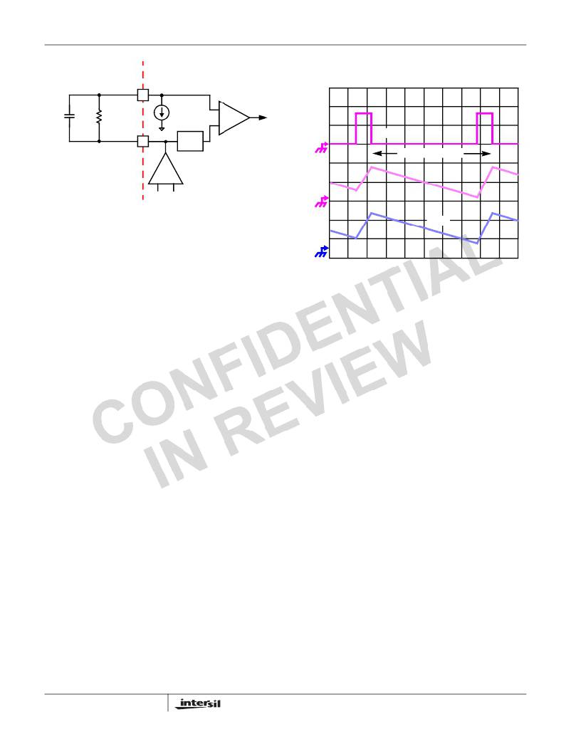
�I� SEN�
�TIME�
�FIGURE� 4.� CONTINUOUS� CURRENT� SAMPLING�
�The� ISL6323B� supports� Inductor� DCR� current� sensing� to�
�continuously� sample� each� channel’s� current� for� channel-current�
�balance.� The� internal� circuitry,� shown� in� Figure� 4� represents�
�Channel� N� of� an� N-Channel� converter.� This� circuitry� is� repeated�
�for� each� channel� in� the� converter,� but� may� not� be� active�
�V� APA� ,� TRIP� =� R� APA� ?� 100� � 10�
�–� 6�
�(EQ.� 4)�
�depending� on� how� many� channels� are� operating.�
�Inductor� windings� have� a� characteristic� distributed�
�PWM� Operation�
�The� timing� of� each� core� channel� is� set� by� the� number� of�
�active� channels.� Channel� detection� on� the� ISEN2-,� ISEN3-�
�and� ISEN4-� pins� selects� 1-Channel� to� 4-Channel� operation�
�for� the� ISL6323B.� The� switching� cycle� is� defined� as� the� time�
�between� PWM� pulse� termination� signals� of� each� channel.�
�resistance� or� DCR� (Direct� Current� Resistance).� For�
�simplicity,� the� inductor� DCR� is� considered� as� a� separate�
�lumped� quantity,� as� shown� in� Figure� 5.� The� channel� current�
�I� Ln� ,� flowing� through� the� inductor,� passes� through� the� DCR.�
�Equation� 5� shows� the� S-domain� equivalent� voltage,� V� L� ,�
�across� the� inductor.�
�V� L� (� s� )� =� I� L� ?� (� s� ?� L� +� DCR� )�
�The� cycle� time� of� the� pulse� signal� is� the� inverse� of� the�
�switching� frequency� set� by� the� resistor� between� the� FS� pin�
�n�
�(EQ.� 5)�
�?� -------------� +� 1� ?�
�?� DCR�
�?�
�(� R� 1� ?� R� 2� )�
�V� C� (� s� )� =� --------------------------------------------------------� ?� K� ?� DCR� ?� I� L�
�and� ground.� The� PWM� signals� command� the� MOSFET�
�driver� to� turn� on/off� the� channel� MOSFETs.�
�For� 4-channel� operation,� the� channel� firing� order� is� 1-2-3-4:�
�PWM3� pulse� happens� 1/4� of� a� cycle� after� PWM4,� PWM2�
�output� follows� another� 1/4� of� a� cycle� after� PWM3,� and�
�PWM1� delays� another� 1/4� of� a� cycle� after� PWM2.� For�
�3-channel� operation,� the� channel� firing� order� is� 1-2-3.�
�Connecting� ISEN4-� to� VCC� selects� three� channel� operation�
�A� simple� R-C� network� across� the� inductor� (R� 1� ,� R� 2� and� C)�
�extracts� the� DCR� voltage,� as� shown� in� Figure� 5.� The� voltage�
�across� the� sense� capacitor,� V� C� ,� can� be� shown� to� be�
�proportional� to� the� channel� current� I� Ln� ,� shown� in� Equation� 6.�
�s� ?� L�
�(EQ.� 6)�
�?� ?� n�
�?� s� ?� ------------------------� ?� C� +� 1� ?�
�?� R� 1� +� R� 2� ?�
�R� 2�
�and� the� pulse� times� are� spaced� in� 1/3� cycle� increments.� If�
�ISEN3-� is� also� connected� to� VCC,� 2-Channel� operation� is�
�selected� and� the� PWM2� pulse� happens� 1/2� of� a� cycle� after�
�PWM1� pulse.� If� ISEN2-� is� also� connected� to� VCC,�
�Where:�
�K� =� ---------------------�
�R� 2� +� R� 1�
�(EQ.� 7)�
�1HChannel� operation� is� selected.�
�Continuous� Current� Sampling�
�In� order� to� realize� proper� current-balance,� the� currents� in�
�each� channel� are� sampled� continuously� every� switching�
�cycle.� During� this� time,� the� current-sense� amplifier� uses� the�
�ISEN� inputs� to� reproduce� a� signal� proportional� to� the�
�14�
�If� the� R-C� network� components� are� selected� such� that� the�
�RC� time� constant� matches� the� inductor� L/DCR� time� constant�
�(see� Equations� 7� and� 8),� then� V� C� is� equal� to� the� voltage� drop�
�across� the� DCR� multiplied� by� the� ratio� of� the� resistor� divider,�
�K.� If� a� resistor� divider� is� not� being� used,� the� value� for� K� is� 1.�
�FN6879.1�
�May� 12,� 2010�
�相关PDF资料 |
PDF描述 |
|---|---|
| RMC26DRTH-S13 | CONN EDGECARD 52POS .100 EXTEND |
| X40015S8I-B | IC VOLTAGE MONITOR DUAL 8-SOIC |
| X40015S8I-AT1 | IC VOLTAGE MONITOR DUAL 8-SOIC |
| ISL6323AIRZ-T | IC PWM CTRLR SYNC BUCK DL 48QFN |
| ACM25DSXN | CONN EDGECARD 50POS DIP .156 SLD |
相关代理商/技术参数 |
参数描述 |
|---|---|
| ISL6323BIRZ-TR5381 | 制造商:Intersil Corporation 功能描述:4+1 PHASE CONT. FOR CORE+NORTHBRIDGE,2 PHASE PSI, 3.4MHZ SVI - Tape and Reel 制造商:Intersil Corporation 功能描述:IC PWM CTRLR SYNC BUCK DL 48QFN 制造商:Intersil 功能描述:4+1 PHS CONT CORE + NORTHBRDG PROG |
| ISL6323CRZ | 功能描述:IC HYBRID CTRLR PWM MONO 48-QFN RoHS:是 类别:集成电路 (IC) >> PMIC - 稳压器 - 专用型 系列:- 标准包装:43 系列:- 应用:控制器,Intel VR11 输入电压:5 V ~ 12 V 输出数:1 输出电压:0.5 V ~ 1.6 V 工作温度:-40°C ~ 85°C 安装类型:表面贴装 封装/外壳:48-VFQFN 裸露焊盘 供应商设备封装:48-QFN(7x7) 包装:管件 |
| ISL6323CRZR5285 | 制造商:Intersil Corporation 功能描述: |
| ISL6323CRZ-T | 功能描述:IC HYBRID CTRLR PWM MONO 48-QFN RoHS:是 类别:集成电路 (IC) >> PMIC - 稳压器 - 专用型 系列:- 标准包装:43 系列:- 应用:控制器,Intel VR11 输入电压:5 V ~ 12 V 输出数:1 输出电压:0.5 V ~ 1.6 V 工作温度:-40°C ~ 85°C 安装类型:表面贴装 封装/外壳:48-VFQFN 裸露焊盘 供应商设备封装:48-QFN(7x7) 包装:管件 |
| ISL6323EVAL1Z | 功能描述:EVAL BOARD 1 FOR ISL6323 RoHS:是 类别:编程器,开发系统 >> 评估板 - DC/DC 与 AC/DC(离线)SMPS 系列:* 产品培训模块:Obsolescence Mitigation Program 标准包装:1 系列:True Shutdown™ 主要目的:DC/DC,步升 输出及类型:1,非隔离 功率 - 输出:- 输出电压:- 电流 - 输出:1A 输入电压:2.5 V ~ 5.5 V 稳压器拓扑结构:升压 频率 - 开关:3MHz 板类型:完全填充 已供物品:板 已用 IC / 零件:MAX8969 |
发布紧急采购,3分钟左右您将得到回复。