参数资料
| 型号: | ISL6334CIRZ-T |
| 厂商: | Intersil |
| 文件页数: | 26/30页 |
| 文件大小: | 0K |
| 描述: | IC CTRLR PWM SYNC BUCK 40-QFN |
| 标准包装: | 4,000 |
| 应用: | 控制器,Intel VR11.1 |
| 输入电压: | 3 V ~ 12 V |
| 输出数: | 1 |
| 输出电压: | 0.5 V ~ 1.6 V |
| 工作温度: | -40°C ~ 85°C |
| 安装类型: | 表面贴装 |
| 封装/外壳: | 40-VFQFN 裸露焊盘 |
| 供应商设备封装: | 40-QFN(6x6) |
| 包装: | 带卷 (TR) |
第1页第2页第3页第4页第5页第6页第7页第8页第9页第10页第11页第12页第13页第14页第15页第16页第17页第18页第19页第20页第21页第22页第23页第24页第25页当前第26页第27页第28页第29页第30页
�� �
�
�ISL6334B,� ISL6334C�
�to� be� 1.2x� the� maximum� load� current� of� the� specific�
�application.�
�With� integrated� temperature� compensation,� the� sensed�
�current� signal� is� independent� on� the� operational� temperature�
�of� the� power� stage,� i.e.� the� temperature� effect� on� the� current�
�sense� element� R� X� is� cancelled� by� the� integrated�
�temperature� compensation� function.� R� X� in� Equation� 29�
�should� be� the� resistance� of� the� current� sense� element� at� the�
�where� N� is� the� active� channel� number,� R� ISEN� is� the� sense�
�resistor� connected� to� the� ISEN+� pin,� and� R� X� is� the�
�resistance� of� the� current� sense� element,� either� the� DCR� of�
�the� inductor� or� R� SENSE� depending� on� the� sensing� method.�
�If� one� or� more� of� the� current� sense� resistors� are� adjusted� for�
�thermal� balance� (as� in� Equation� 30),� the� load-line� regulation�
�resistor� should� be� selected� based� on� the� average� value� of�
�the� current� sensing� resistors,� as� given� in� Equation� 33:�
�R� X�
�room� temperature.�
�When� the� integrated� temperature� compensation� function� is�
�R� LL�
�R� FB� =� ----------�
�∑� R� ISEN� (� n� )�
�n�
�(EQ.� 33)�
�disabled� by� pulling� the� TCOMP� pin� to� GND,� the� sensed�
�current� will� be� dependent� on� the� operational� temperature� of�
�the� power� stage,� since� the� DC� resistance� of� the� current�
�sense� element� may� be� changed� according� to� the� operational�
�temperature.� R� X� in� Equation� 29� should� be� the� maximum� DC�
�resistance� of� the� current� sense� element� at� the� all� operational�
�temperature.�
�In� certain� circumstances,� it� may� be� necessary� to� adjust� the�
�value� of� one� or� more� ISEN� resistors.� When� the� components�
�of� one� or� more� channels� are� inhibited� from� effectively�
�dissipating� their� heat� so� that� the� affected� channels� run� hotter�
�than� desired,� choose� new,� smaller� values� of� RISEN� for� the�
�affected� phases� (see� the� section� entitled� “Channel-Current�
��desired� decrease� in� temperature� rise� in� order� to� cause�
�proportionally� less� current� to� flow� in� the� hotter� phase,� as�
�shown� in� Equation� 30:�
�where� R� ISEN(n)� is� the� current� sensing� resistor� connected� to�
�the� n� th� ISEN+� pin.�
�Compensation�
�The� two� opposing� goals� of� compensating� the� voltage�
�regulator� are� stability� and� speed.� Depending� on� whether� the�
�regulator� employs� the� optional� load-line� regulation� as�
�described� in� Load-Line� Regulation,� there� are� two� distinct�
�methods� for� achieving� these� goals.�
�COMPENSATING� LOAD-LINE� REGULATED�
�CONVERTER�
�The� load-line� regulated� converter� behaves� in� a� similar�
�manner� to� a� peak-current� mode� controller� because� the� two�
�poles� at� the� output-filter� L-C� resonant� frequency� split� with�
�the� introduction� of� current� information� into� the� control� loop.�
�The� final� location� of� these� poles� is� determined� by� the� system�
�function,� the� gain� of� the� current� signal,� and� the� value� of� the�
�R� ISEN� ,� 2� =� R� ISEN� ----------� 2�
�Δ� T�
�Δ� T� 1�
�(EQ.� 30)�
�compensation� components,� R� C� and� C� C� .�
�Since� the� system� poles� and� zero� are� affected� by� the� values�
�In� Equation� 30,� make� sure� that� Δ� T� 2� is� the� desired� temperature�
�rise� above� the� ambient� temperature,� and� Δ� T� 1� is� the� measured�
�temperature� rise� above� the� ambient� temperature.� While� a�
�single� adjustment� according� to� Equation� 30� is� usually�
�sufficient,� it� may� occasionally� be� necessary� to� adjust� R� ISEN�
�two� or� more� times� to� achieve� optimal� thermal� balance�
�between� all� channels.�
�Load-Line� Regulation� Resistor�
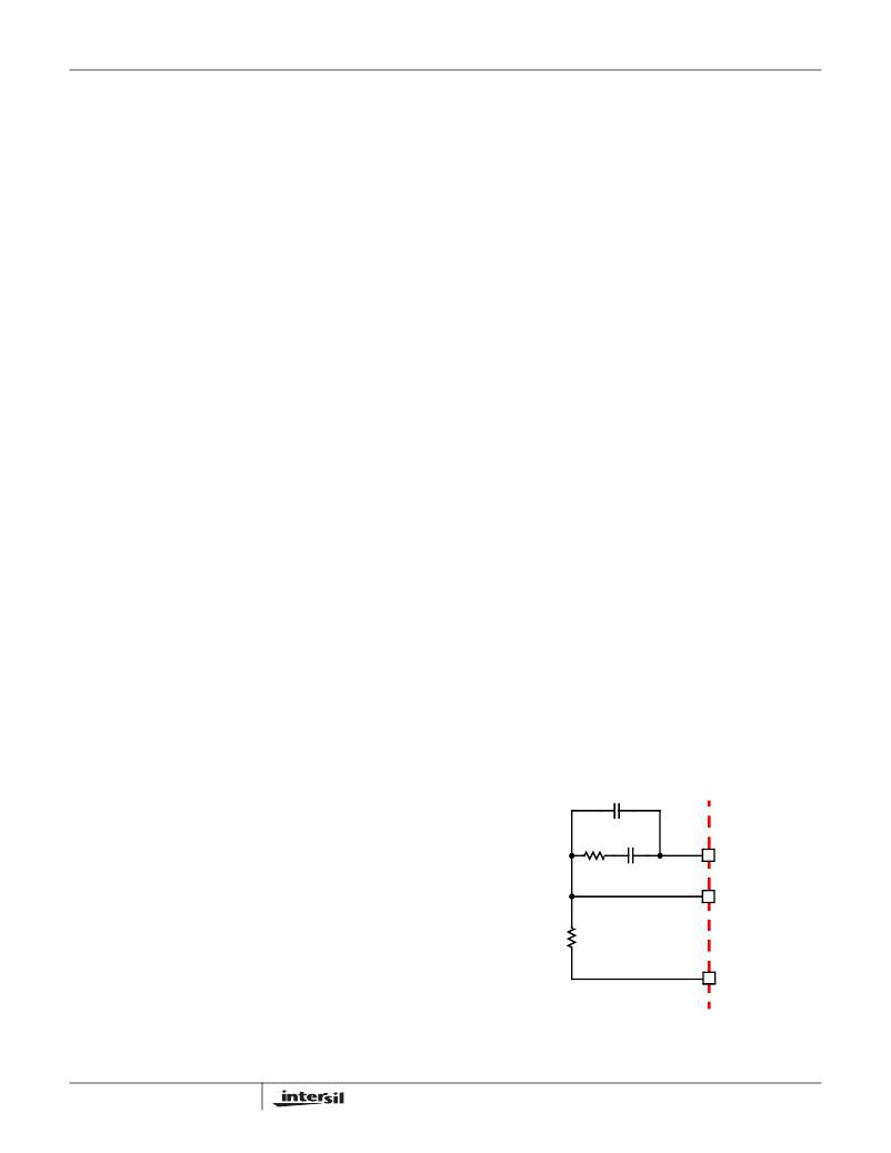
�The� load-line� regulation� resistor� is� labelled� R� FB� in� Figure� 6.�
�Its� value� depends� on� the� desired� loadline� requirement� of� the�
�of� the� components� that� are� meant� to� compensate� them,� the�
�solution� to� the� system� equation� becomes� fairly� complicated.�
�Fortunately� there� is� a� simple� approximation� that� comes� very�
�close� to� an� optimal� solution.� Treating� the� system� as� though� it�
�were� a� voltage-mode� regulator� by� compensating� the� L-C�
�poles� and� the� ESR� zero� of� the� voltage-mode� approximation�
�yields� a� solution� that� is� always� stable� with� very� close� to� ideal�
�transient� performance.�
�C� 2� (OPTIONAL)�
�I� FL�
�application.�
�The� desired� loadline� can� be� calculated� using� Equation� 31:�
�V� DROOP�
�R� LL� =� -------------------------�
�(EQ.� 31)�
�where� I� FL� is� the� full� load� current� of� the� specific� application,�
�and� VR� DROOP� is� the� desired� voltage� droop� under� the� full�
�load� condition.�
�R� FB�
�R� C�
�+�
�V� DROOP�
�-�
�C� C�
�COMP�
�FB�
�VDIFF�
�Based� on� the� desired� loadline� R� LL� ,� the� loadline� regulation�
�resistor� can� be� calculated� using� Equation� 32:�
�NR� R�
�R� FB� =� ----------------------------------�
�ISEN� LL�
�R� X�
�26�
�(EQ.� 32)�
�FIGURE� 17.� COMPENSATION� CONFIGURATION� FOR�
�LOAD-LINE� REGULATED� ISL6334B,� ISL6334C�
�CIRCUIT�
�FN6689.2�
�August� 31,� 2010�
�相关PDF资料 |
PDF描述 |
|---|---|
| RMM30DRSD-S288 | CONN EDGECARD 60POS .156 EXTEND |
| EYM40DRST | CONN EDGECARD 80POS DIP .156 SLD |
| X40031S14I-BT1 | IC VOLTAGE MONITOR TRPL 14-SOIC |
| RMM15DRMD | CONN EDGECARD 30POS .156 WW |
| EGM40DRST | CONN EDGECARD 80POS DIP .156 SLD |
相关代理商/技术参数 |
参数描述 |
|---|---|
| ISL6334CRZ | 功能描述:IC CTRLR PWM 4PHASE BUCK 40-QFN RoHS:是 类别:集成电路 (IC) >> PMIC - 稳压器 - 专用型 系列:- 标准包装:43 系列:- 应用:控制器,Intel VR11 输入电压:5 V ~ 12 V 输出数:1 输出电压:0.5 V ~ 1.6 V 工作温度:-40°C ~ 85°C 安装类型:表面贴装 封装/外壳:48-VFQFN 裸露焊盘 供应商设备封装:48-QFN(7x7) 包装:管件 |
| ISL6334CRZ-T | 功能描述:IC CTRLR PWM 4PHASE BUCK 40-QFN RoHS:是 类别:集成电路 (IC) >> PMIC - 稳压器 - 专用型 系列:- 标准包装:43 系列:- 应用:控制器,Intel VR11 输入电压:5 V ~ 12 V 输出数:1 输出电压:0.5 V ~ 1.6 V 工作温度:-40°C ~ 85°C 安装类型:表面贴装 封装/外壳:48-VFQFN 裸露焊盘 供应商设备封装:48-QFN(7x7) 包装:管件 |
| ISL6334DCRZ | 功能描述:IC CTRLR PWM 4PHASE VR11.1 40QFN RoHS:是 类别:集成电路 (IC) >> PMIC - 稳压器 - 专用型 系列:- 标准包装:43 系列:- 应用:控制器,Intel VR11 输入电压:5 V ~ 12 V 输出数:1 输出电压:0.5 V ~ 1.6 V 工作温度:-40°C ~ 85°C 安装类型:表面贴装 封装/外壳:48-VFQFN 裸露焊盘 供应商设备封装:48-QFN(7x7) 包装:管件 |
| ISL6334DCRZ-T | 功能描述:IC CTRLR PWM 4PHASE VR11.1 40QFN RoHS:是 类别:集成电路 (IC) >> PMIC - 稳压器 - 专用型 系列:- 标准包装:43 系列:- 应用:控制器,Intel VR11 输入电压:5 V ~ 12 V 输出数:1 输出电压:0.5 V ~ 1.6 V 工作温度:-40°C ~ 85°C 安装类型:表面贴装 封装/外壳:48-VFQFN 裸露焊盘 供应商设备封装:48-QFN(7x7) 包装:管件 |
| ISL6334DIRZ | 功能描述:IC CTRLR PWM 4PHASE VR11.1 40QFN RoHS:是 类别:集成电路 (IC) >> PMIC - 稳压器 - 专用型 系列:- 标准包装:43 系列:- 应用:控制器,Intel VR11 输入电压:5 V ~ 12 V 输出数:1 输出电压:0.5 V ~ 1.6 V 工作温度:-40°C ~ 85°C 安装类型:表面贴装 封装/外壳:48-VFQFN 裸露焊盘 供应商设备封装:48-QFN(7x7) 包装:管件 |
发布紧急采购,3分钟左右您将得到回复。