- 您现在的位置:买卖IC网 > PDF目录19908 > ISL6412IRZ (Intersil)IC REG LDO 1.8V/2.8V/2.8V 16-QFN PDF资料下载
参数资料
| 型号: | ISL6412IRZ |
| 厂商: | Intersil |
| 文件页数: | 8/10页 |
| 文件大小: | 0K |
| 描述: | IC REG LDO 1.8V/2.8V/2.8V 16-QFN |
| 标准包装: | 750 |
| 稳压器拓扑结构: | 正,固定式 |
| 输出电压: | 1.8V,2.8V,2.8V |
| 输入电压: | 3 V ~ 3.6 V |
| 电压 - 压降(标准): | -,0.125V @ 225mA,0.1V @ 125mA |
| 稳压器数量: | 3 |
| 电流 - 输出: | 330mA(最小),225mA(最小),125mA(最小) |
| 电流 - 限制(最小): | 500mA,330mA,300mA |
| 工作温度: | -40°C ~ 85°C |
| 安装类型: | 表面贴装 |
| 封装/外壳: | 16-VQFN 裸露焊盘 |
| 供应商设备封装: | 16-QFN-EP(4x4) |
| 包装: | 管件 |
�� �
�
�ISL6412�
�pin� also� goes� LOW� during� thermal� shutdown� or� an�
�overcurrent� event� on� LDO1.� Connect� this� pin� to� GND,� if�
�unused.�
�RESET� -� This� pin� is� the� active-LOW� output� of� the� push-pull�
�output� stage� of� the� integrated� reset� supervisory� circuit.� The�
�reset� circuit� monitors� V� IN� and� asserts� a� RESET� output� at� this�
�pin,� if� V� IN� falls� below� the� RESET� threshold.� The� RESET�
�output� remains� LOW,� while� the� V� IN� pin� voltage� is� below� the�
�reset� threshold,� and� for� at� least� 25ms,� after� V� IN� rises� above�
�the� RESET� threshold.�
�Functional� Description�
�The� ISL6412� is� a� 3-in-1� multi-output,� low� dropout,� regulator�
�designed� for� wireless� chipset� power� applications.� It� supplies�
�three� fixed� output� voltages� 1.8V,� 2.8V� and� 2.8V.� Each� LDO�
�consists� of� a� 1.2V� reference,� error� amplifier,� MOSFET� driver,�
�P-Channel� pass� transistor,� dual-mode� comparator� and�
�internal� feedback� voltage� divider.�
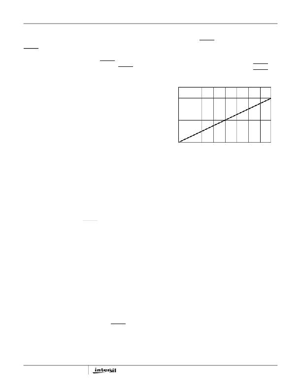
�The� voltage� at� the� CT� pin� is� compared� to� the� 1.2V� bandgap�
�voltage.� The� charging� of� the� CT� capacitor� behaves� like� an�
�RC� network� and� the� RESET� delay� can� be� approximated� by:�
�Td� =� -R*C*ln(1-1.2V/VIN)�
�Where� C� is� the� capacitor� at� CT,� and� R� is� 11.1M� Ω� for�
�VIN� =� 3.3V.� With� no� capacitor� on� the� CT� pin� the� RESET�
�delay� will� be� close� to� zero.� Figure� 12� shows� the� RESET�
�delay� vs� CT� capacitance.�
�500�
�400�
�300�
�200�
�100�
�The� 1.2V� band� gap� reference� is� connected� to� the� error�
�0�
�0�
�0.01�
�0.02�
�0.03�
�0.04�
�0.05�
�0.06�
�0.07�
�0�
�amplifier’s� inverting� input.� The� error� amplifier� compares� this�
�reference� to� the� selected� feedback� voltage� and� amplifies� the�
�difference.� The� MOSFET� driver� reads� the� error� signal� and�
�applies� the� appropriate� drive� to� the� P-Channel� pass� transistor.�
�If� the� feedback� voltage� is� lower� then� the� reference� voltage,� the�
�pass� transistor� gate� is� pulled� lower,� allowing� more� current� to�
�pass� and� increasing� the� output� voltage.� If� the� feedback�
�voltage� is� higher� then� the� reference� voltage,� the� pass�
�transistor� gate� is� driven� higher,� allowing� less� current� to� pass� to�
�the� output.� The� output� voltage� is� fed� back� through� an� internal�
�resistor� divider� connected� to� OUT1/OUT2/OUT3� pins.�
�Additional� blocks� include� an� output� overcurrent� protection,�
�thermal� sensor,� fault� detector,� RESET� function� and�
�shutdown� logic.�
�Internal� P-Channel� Pass� Transistors�
�The� ISL6412� features� a� typical� 0.5� Ω� r� DS(ON)� P-channel�
�MOSFET� pass� transistors.� This� provides� several� advantages�
�over� similar� designs� using� PNP� bipolar� pass� transistors.� The�
�P-Channel� MOSFET� requires� no� base� drive,� which� reduces�
�quiescent� current� considerably.� PNP� based� regulators� waste�
�considerable� current� in� dropout� when� the� pass� transistor�
�saturates.� They� also� use� high� base� drive� currents� under�
�large� loads.� The� ISL6412� does� not� suffer� from� these�
�problems.�
�Integrated� Reset� for� MAC/Baseband� Processors�
�The� ISL6412� includes� a� microprocessor� supervisory� block.�
�This� block� eliminates� the� extra� reset� IC� and� external�
�components� needed� in� wireless� chipset� applications.� This�
�block� performs� a� single� function;� it� asserts� a� RESET� signal�
�whenever� the� V� IN� supply� voltage� decreases� below� a� preset�
�threshold,� keeping� it� asserted� for� a� programmable� time� (set�
�by� external� capacitor� CT)� after� the� V� IN� pin� voltage� has� risen�
�above� the� reset� threshold.� The� reset� threshold� for� the�
�ISL6412� is� 2.63V� typical.�
�8�
�CT� (μF)�
�FIGURE� 12.� RESET� DELAY� vs� CT� CAPACITANCE�
�Output� Voltages�
�The� ISL6412� provides� fixed� output� voltages� for� use� in�
�Wireless� Chipset� applications.� Internal� trimmed� resistor�
�networks� set� the� typical� output� voltages� as� shown� here:�
�V� OUT1� =� 1.8V;� V� OUT2� =� 2.8V;� V� OUT3� =� 2.8V.�
�Shutdown�
�Pulling� the� SHDN� pin� LOW� puts� the� complete� chip� into�
�shutdown� mode,� and� supply� current� drops� to� 5� μ� A� typical.�
�This� input� has� an� internal� pull-up� resistor,� so� that� in� normal�
�operation� the� outputs� are� always� enabled;� external� pull-up�
�resistors� are� not� required.�
�Current� Limit�
�The� ISL6412� monitors� and� controls� the� pass� transistor� ’s�
�gate� voltage� to� limit� the� output� current.� The� current� limit� for�
�LDO1� is� 500mA,� LDO2� is� 330mA� and� LDO3� is� 300mA.� The�
�output� can� be� shorted� to� ground� without� damaging� the� part�
�due� to� the� current� limit� and� thermal� protection� features.�
�FN9067.1�
�March� 20,� 2007�
�相关PDF资料 |
PDF描述 |
|---|---|
| LTC4301IDD#TRPBF | IC BUFFER BUS HOTSWAP 2WR 8DFN |
| V24C36H100B3 | CONVERTER MOD DC/DC 36V 100W |
| ESM08DRMS | CONN EDGECARD 16POS .156 WW |
| V48C5H100BF3 | CONVERTER MOD DC/DC 5V 100W |
| RBC12DREH-S13 | CONN EDGECARD 24POS .100 EXTEND |
相关代理商/技术参数 |
参数描述 |
|---|---|
| ISL6412IRZ-TK | 功能描述:低压差稳压器 - LDO VER OF ISL6412IR-T 1 000 PC RoHS:否 制造商:Texas Instruments 最大输入电压:36 V 输出电压:1.4 V to 20.5 V 回动电压(最大值):307 mV 输出电流:1 A 负载调节:0.3 % 输出端数量: 输出类型:Fixed 最大工作温度:+ 125 C 安装风格:SMD/SMT 封装 / 箱体:VQFN-20 |
| ISL6413EVAL1 | 功能描述:EVALUATION BOARD ISL6413 RoHS:否 类别:编程器,开发系统 >> 过时/停产零件编号 系列:- 标准包装:1 系列:- 传感器类型:CMOS 成像,彩色(RGB) 传感范围:WVGA 接口:I²C 灵敏度:60 fps 电源电压:5.7 V ~ 6.3 V 嵌入式:否 已供物品:成像器板 已用 IC / 零件:KAC-00401 相关产品:4H2099-ND - SENSOR IMAGE WVGA COLOR 48-PQFP4H2094-ND - SENSOR IMAGE WVGA MONO 48-PQFP |
| ISL6413IR | 功能描述:IC REG TRPL BCK/LINEAR 24-QFN RoHS:否 类别:集成电路 (IC) >> PMIC - 稳压器 - 线性 + 切换式 系列:- 标准包装:2,500 系列:- 拓扑:降压(降压)同步(3),线性(LDO)(2) 功能:任何功能 输出数:5 频率 - 开关:300kHz 电压/电流 - 输出 1:控制器 电压/电流 - 输出 2:控制器 电压/电流 - 输出 3:控制器 带 LED 驱动器:无 带监控器:无 带序列发生器:是 电源电压:5.6 V ~ 24 V 工作温度:-40°C ~ 85°C 安装类型:* 封装/外壳:* 供应商设备封装:* 包装:* |
| ISL6413IR-T5K | 功能描述:IC REG TRPL BCK/LINEAR 24-QFN RoHS:否 类别:集成电路 (IC) >> PMIC - 稳压器 - 线性 + 切换式 系列:- 标准包装:2,500 系列:- 拓扑:降压(降压)同步(3),线性(LDO)(2) 功能:任何功能 输出数:5 频率 - 开关:300kHz 电压/电流 - 输出 1:控制器 电压/电流 - 输出 2:控制器 电压/电流 - 输出 3:控制器 带 LED 驱动器:无 带监控器:无 带序列发生器:是 电源电压:5.6 V ~ 24 V 工作温度:-40°C ~ 85°C 安装类型:* 封装/外壳:* 供应商设备封装:* 包装:* |
| ISL6413IR-TK | 功能描述:IC REG TRPL BCK/LINEAR 24-QFN RoHS:否 类别:集成电路 (IC) >> PMIC - 稳压器 - 线性 + 切换式 系列:- 标准包装:2,500 系列:- 拓扑:降压(降压)同步(3),线性(LDO)(2) 功能:任何功能 输出数:5 频率 - 开关:300kHz 电压/电流 - 输出 1:控制器 电压/电流 - 输出 2:控制器 电压/电流 - 输出 3:控制器 带 LED 驱动器:无 带监控器:无 带序列发生器:是 电源电压:5.6 V ~ 24 V 工作温度:-40°C ~ 85°C 安装类型:* 封装/外壳:* 供应商设备封装:* 包装:* |
发布紧急采购,3分钟左右您将得到回复。