- 您现在的位置:买卖IC网 > PDF目录15194 > ISL6439IRZ-T (Intersil)IC REG CTRLR BUCK PWM VM 16-QFN PDF资料下载
参数资料
| 型号: | ISL6439IRZ-T |
| 厂商: | Intersil |
| 文件页数: | 9/15页 |
| 文件大小: | 0K |
| 描述: | IC REG CTRLR BUCK PWM VM 16-QFN |
| 标准包装: | 6,000 |
| PWM 型: | 电压模式 |
| 输出数: | 1 |
| 频率 - 最大: | 340kHz |
| 占空比: | 100% |
| 电源电压: | 3.3 V ~ 5 V |
| 降压: | 是 |
| 升压: | 无 |
| 回扫: | 无 |
| 反相: | 无 |
| 倍增器: | 无 |
| 除法器: | 无 |
| Cuk: | 无 |
| 隔离: | 无 |
| 工作温度: | -40°C ~ 85°C |
| 封装/外壳: | 16-VQFN 裸露焊盘 |
| 包装: | 带卷 (TR) |
�� �
�
�ISL6439,� ISL6439A�
�that� there� is� a� path� for� the� current� to� flow� other� than� the�
�capacitance� on� the� rail� will� prevent� this� failure� mode.�
�Application� Guidelines�
�Layout� Considerations�
�Layout� is� very� important� in� high� frequency� switching�
�converter� design.� With� power� devices� switching� efficiently� at�
�300kHz� or� 600kHz,� the� resulting� current� transitions� from� one�
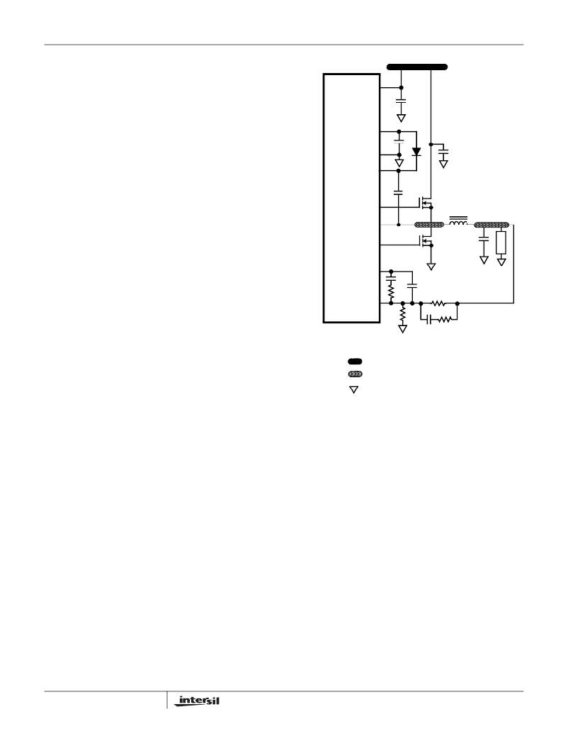
�ISL6439�
�VCC�
�CPVOUT�
�C� VCC�
�+3.3V� V� IN�
�device� to� another� cause� voltage� spikes� across� the�
�interconnecting� impedances� and� parasitic� circuit� elements.�
�GND�
�C� BP�
�D1�
�C� IN�
�These� voltage� spikes� can� degrade� efficiency,� radiate� noise�
�BOOT�
�into� the� circuit,� and� lead� to� device� overvoltage� stress.�
�Careful� component� layout� and� printed� circuit� board� design�
�minimizes� the� voltage� spikes� in� the� converters.�
�As� an� example,� consider� the� turn-off� transition� of� the� PWM�
�MOSFET.� Prior� to� turn-off,� the� MOSFET� is� carrying� the� full� load�
�current.� During� turn-off,� current� stops� flowing� in� the� MOSFET�
�UGATE�
�PHASE�
�LGATE�
�C� BOOT�
�PHASE�
�Q1�
�Q2�
�L� OUT�
�C� OUT�
�V� OUT�
�and� is� picked� up� by� the� lower� MOSFET.� Any� parasitic�
�inductance� in� the� switched� current� path� generates� a� large�
�voltage� spike� during� the� switching� interval.� Careful� component�
�COMP�
�C� 2�
�selection,� tight� layout� of� the� critical� components,� and� short,� wide�
�traces� minimizes� the� magnitude� of� voltage� spikes.�
�There� are� two� sets� of� critical� components� in� a� DC/DC�
�FB�
�R� 2�
�R4�
�C� 1�
�R� 1�
�C� 3� R� 3�
�converter� using� the� ISL6439.� The� switching� components� are�
�the� most� critical� because� they� switch� large� amounts� of�
�energy,� and� therefore� tend� to� generate� large� amounts� of�
�noise.� Next� are� the� small� signal� components� which� connect�
�to� sensitive� nodes� or� supply� critical� bypass� current� and�
�signal� coupling.�
�A� multi-layer� printed� circuit� board� is� recommended.� Figure� 4�
�shows� the� connections� of� the� critical� components� in� the�
�converter.� Note� that� capacitors� C� IN� and� C� OUT� could� each�
�represent� numerous� physical� capacitors.� Dedicate� one� solid�
�layer,� usually� a� middle� layer� of� the� PC� board,� for� a� ground�
�plane� and� make� all� critical� component� ground� connections�
�with� vias� to� this� layer.� Dedicate� another� solid� layer� as� a�
�power� plane� and� break� this� plane� into� smaller� islands� of�
�common� voltage� levels.� Keep� the� metal� runs� from� the�
�PHASE� terminals� to� the� output� inductor� short.� The� power�
�plane� should� support� the� input� power� and� output� power�
�nodes.� Use� copper� filled� polygons� on� the� top� and� bottom�
�circuit� layers� for� the� phase� nodes.� Use� the� remaining� printed�
�circuit� layers� for� small� signal� wiring.� The� wiring� traces� from�
�the� GATE� pins� to� the� MOSFET� gates� should� be� kept� short�
�and� wide� enough� to� easily� handle� the� 1A� of� drive� current.�
�The� switching� components� should� be� placed� close� to� the�
�ISL6439� first.� Minimize� the� length� of� the� connections� between�
�the� input� capacitors,� C� IN� ,� and� the� power� switches� by� placing�
�them� nearby.� Position� both� the� ceramic� and� bulk� input�
�capacitors� as� close� to� the� upper� MOSFET� drain� as� possible.�
�Position� the� output� inductor� and� output� capacitors� between� the�
�upper� MOSFET� and� lower� MOSFET� and� the� load.�
�9�
�KEY�
�ISLAND� ON� POWER� PLANE� LAYER�
�ISLAND� ON� CIRCUIT� PLANE� LAYER�
�VIA� CONNECTION� TO� GROUND� PLANE�
�FIGURE� 4.� PRINTED� CIRCUIT� BOARD� POWER� PLANES�
�AND� ISLANDS�
�The� critical� small� signal� components� include� any� bypass�
�capacitors,� feedback� components,� and� compensation�
�components.� Position� the� bypass� capacitor,� C� BP� ,� close� to�
�the� VCC� pin� with� a� via� directly� to� the� ground� plane.� Place� the�
�PWM� converter� compensation� components� close� to� the� FB�
�and� COMP� pins.� The� feedback� resistors� for� both� regulators�
�should� also� be� located� as� close� as� possible� to� the� relevant�
�FB� pin� with� vias� tied� straight� to� the� ground� plane� as� required.�
�Feedback� Compensation�
�Figure� 5� highlights� the� voltage-mode� control� loop� for� a�
�synchronous-rectified� buck� converter.� The� output� voltage�
�(V� OUT� )� is� regulated� to� the� Reference� voltage� level.� The�
�error� amplifier� (Error� Amp)� output� (V� E/A� )� is� compared� with�
�the� oscillator� (OSC)� triangular� wave� to� provide� a� pulse-�
�width� modulated� (PWM)� wave� with� an� amplitude� of� V� IN� at�
�the� PHASE� node.� The� PWM� wave� is� smoothed� by� the� output�
�filter� (L� O� and� C� O� ).�
�The� modulator� transfer� function� is� the� small-signal� transfer�
�function� of� V� OUT� /V� E/A� .� This� function� is� dominated� by� a� DC�
�Gain� and� the� output� filter� (L� O� and� C� O� ),� with� a� double� pole�
�break� frequency� at� F� LC� and� a� zero� at� F� ESR� .� The� DC� Gain� of�
�FN9057.5�
�November� 5,� 2008�
�相关PDF资料 |
PDF描述 |
|---|---|
| RSC12DRES-S93 | CONN EDGECARD 24POS .100 EYELET |
| ISL6439AIRZ-T | IC REG CTRLR BUCK PWM VM 16-QFN |
| ISL6545CRZ-TS2694 | IC REG CTRLR BUCK PWM VM 10-DFN |
| ISL88002IE26Z-TK | IC VOLT SUPERVISOR 2.63V SC-70 |
| ISL6545CRZ-T | IC REG CTRLR BUCK PWM VM 10-DFN |
相关代理商/技术参数 |
参数描述 |
|---|---|
| ISL6440ACB WAF | 制造商:Harris Corporation 功能描述: |
| ISL6440ACB-T | 制造商:Rochester Electronics LLC 功能描述:- Bulk |
| ISL6440EVAL1 | 制造商:Intersil Corporation 功能描述:EVAL BD FOR ISL6440 - Bulk |
| ISL6440EVAL1Z | 功能描述:EVALUATION BOARD FOR ISL6440 RoHS:是 类别:编程器,开发系统 >> 评估板 - DC/DC 与 AC/DC(离线)SMPS 系列:- 产品培训模块:Obsolescence Mitigation Program 标准包装:1 系列:True Shutdown™ 主要目的:DC/DC,步升 输出及类型:1,非隔离 功率 - 输出:- 输出电压:- 电流 - 输出:1A 输入电压:2.5 V ~ 5.5 V 稳压器拓扑结构:升压 频率 - 开关:3MHz 板类型:完全填充 已供物品:板 已用 IC / 零件:MAX8969 |
| ISL6440IA | 功能描述:IC REG CTRLR BUCK PWM CM 24-QSOP RoHS:否 类别:集成电路 (IC) >> PMIC - 稳压器 - DC DC 切换控制器 系列:- 标准包装:4,000 系列:- PWM 型:电压模式 输出数:1 频率 - 最大:1.5MHz 占空比:66.7% 电源电压:4.75 V ~ 5.25 V 降压:是 升压:无 回扫:无 反相:无 倍增器:无 除法器:无 Cuk:无 隔离:无 工作温度:-40°C ~ 85°C 封装/外壳:40-VFQFN 裸露焊盘 包装:带卷 (TR) |
发布紧急采购,3分钟左右您将得到回复。