- 您现在的位置:买卖IC网 > PDF目录15180 > ISL6440IAZ-TK (Intersil)IC REG CTRLR BUCK PWM CM 24-QSOP PDF资料下载
参数资料
| 型号: | ISL6440IAZ-TK |
| 厂商: | Intersil |
| 文件页数: | 10/15页 |
| 文件大小: | 0K |
| 描述: | IC REG CTRLR BUCK PWM CM 24-QSOP |
| 产品培训模块: | Solutions for Industrial Control Applications |
| 标准包装: | 1,000 |
| PWM 型: | 电流模式 |
| 输出数: | 2 |
| 频率 - 最大: | 340kHz |
| 占空比: | 93% |
| 电源电压: | 4.5 V ~ 24 V |
| 降压: | 是 |
| 升压: | 无 |
| 回扫: | 无 |
| 反相: | 无 |
| 倍增器: | 无 |
| 除法器: | 无 |
| Cuk: | 无 |
| 隔离: | 无 |
| 工作温度: | -40°C ~ 85°C |
| 封装/外壳: | 24-SSOP(0.154",3.90mm 宽) |
| 包装: | 带卷 (TR) |
�� �
�
�ISL6440�
�Input� Voltage� Range�
�V� IN� (� min� )� =� ?� --------------------------------� ?� +� V� d2� –� V� d1�
�The� ISL6440� is� designed� to� operate� from� input� supplies�
�ranging� from� 4.5V� to� 24V.� However,� the� input� voltage� range�
�can� be� effectively� limited� by� the� available� maximum� duty�
�cycle� (D� MAX� =� 93%).�
�V� OUT� +� V� d1�
�?� 0.93� ?�
�where,�
�Vd1� =� Sum� of� the� parasitic� voltage� drops� in� the� inductor�
�discharge� path,� including� the� lower� FET,� inductor� and� PC�
�board.�
�Vd2� =� Sum� of� the� voltage� drops� in� the� charging� path,�
�VCC5�
�BOOT�
�UGATE�
�PHASE�
�ISL6440�
�VIN�
�V� IN� (� max� )� ≤� ----------------------------------------------------�
�(� 7� )� (� R� CS� )�
�(� I� OC� )� (� R� DS� (� on� )� )�
�including� the� upper� FET,� inductor� and� PC� board� resistances.�
�The� maximum� input� voltage� and� minimum� output� voltage� is�
�limited� by� the� minimum� on-time� (t� ON(min)� ).�
�V� OUT�
�t� ON� (� min� )� � 300kHz�
�where,� t� ON(min)� =� 30ns�
�Gate� Control� Logic�
�The� gate� control� logic� translates� generated� PWM� signals�
�into� gate� drive� signals� providing� amplification,� level� shifting�
�and� shoot-through� protection.� The� gate� drivers� have� some�
�circuitry� that� helps� optimize� the� ICs� performance� over� a� wide�
�range� of� operational� conditions.� As� MOSFET� switching�
�times� can� vary� dramatically� from� type� to� type� and� with� input�
�voltage,� the� gate� control� logic� provides� adaptive� dead� time�
�by� monitoring� real� gate� waveforms� of� both� the� upper� and� the�
�lower� MOSFETs.� Shoot-through� control� logic� provides� a�
�20ns� deadtime� to� ensure� that� both� the� upper� and� lower�
�MOSFETs� will� not� turn� on� simultaneously� and� cause� a� shoot-�
�through� condition.�
�Gate� Drivers�
�The� low-side� gate� driver� is� supplied� from� VCC5� and� provides�
�a� peak� sink/source� current� of� 400mA.� The� high-side� gate�
�driver� is� also� capable� of� 400mA� current.� Gate-drive� voltages�
�for� the� upper� N-Channel� MOSFET� are� generated� by� the�
�flying� capacitor� boot� circuit.� A� boot� capacitor� connected� from�
�the� BOOT� pin� to� the� PHASE� node� provides� power� to� the�
�high� side� MOSFET� driver.� To� limit� the� peak� current� in� the� IC,�
�an� external� resistor� may� be� placed� between� the� UGATE� pin�
�and� the� gate� of� the� external� MOSFET.� This� small� series�
�resistor� also� damps� any� oscillations� caused� by� the� resonant�
�tank� of� the� parasitic� inductances� in� the� traces� of� the� board�
�and� the� FET’s� gate� to� drain� capacitance.�
�10�
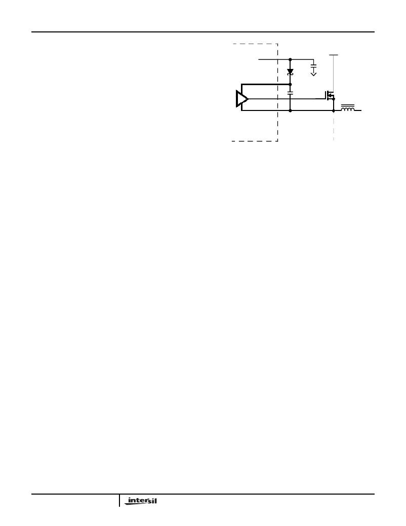
�FIGURE� 15.�
�At� start-up� the� low-side� MOSFET� turns� on� and� forces�
�PHASE� to� ground� in� order� to� charge� the� BOOT� capacitor� to�
�5V.� After� the� low-side� MOSFET� turns� off,� the� high-side�
�MOSFET� is� turned� on� by� closing� an� internal� switch� between�
�BOOT� and� UGATE.� This� provides� the� necessary� gate-to-�
�source� voltage� to� turn� on� the� upper� MOSFET,� an� action� that�
�boosts� the� 5V� gate� drive� signal� above� VIN.� The� current�
�required� to� drive� the� upper� MOSFET� is� drawn� from� the�
�internal� 5V� regulator.�
�Protection� Circuits�
�The� converter� output� is� monitored� and� protected� against�
�overload,� short� circuit� and� undervoltage� conditions.� A�
�sustained� overload� on� the� output� sets� the� PGOOD� low� and�
�initiates� hiccup� mode.�
�Both� PWM� controllers� use� the� lower� MOSFET’s� on-�
�resistance,� r� DS(ON)� ,� to� monitor� the� current� in� the� converter.�
�The� sensed� voltage� drop� is� compared� with� a� threshold� set� by�
�a� resistor� connected� from� the� OCSETx� pin� to� ground.�
�R� OCSET� =� -------------------------------------------�
�where,� I� OC� is� the� desired� overcurrent� protection� threshold,�
�and� R� CS� is� a� value� of� the� current� sense� resistor� connected�
�to� the� ISENx� pin.� If� the� lower� MOSFET� current� exceeds� the�
�overcurrent� threshold,� an� overcurrent� condition� is� detected.�
�If� overcurrent� is� detected� for� 2� consecutive� clock� cycles� then�
�the� IC� enters� a� hiccup� mode� by� turning� off� the� gate� drivers�
�and� entering� into� soft-start.� The� IC� will� cycle� 2� times� through�
�soft-start� before� trying� to� restart.� The� IC� will� continue� to� cycle�
�through� soft-start� until� the� overcurrent� condition� is� removed.�
�Because� of� the� nature� of� this� current� sensing� technique,� and�
�to� accommodate� a� wide� range� of� r� DS(ON)� variations,� the�
�value� of� the� overcurrent� threshold� should� represent� an�
�overload� current� about� 150%� to� 180%� of� the� maximum�
�operating� current.� If� more� accurate� current� protection� is�
�desired� place� a� current� sense� resistor� in� series� with� the�
�lower� MOSFET� source.�
�FN9040.2�
�October� 4,� 2005�
�相关PDF资料 |
PDF描述 |
|---|---|
| VE-25P-EY-F4 | CONVERTER MOD DC/DC 13.8V 50W |
| SH472M010ST | CAP ALUM 4700UF 10V 20% RADIAL |
| H2ABT-10110-W4-ND | JUMPER-H1502TR/A2015W/H1500TR10" |
| VI-B4J-EV-F3 | CONVERTER MOD DC/DC 36V 150W |
| CAT706ZI-GT3 | IC SUPERVISOR CIRCUIT 8-MSOP |
相关代理商/技术参数 |
参数描述 |
|---|---|
| ISL6441IR | 功能描述:IC CTRLR SGL/STEP DOWN PWM 28QFN RoHS:否 类别:集成电路 (IC) >> PMIC - 电源管理 - 专用 系列:- 应用说明:Ultrasound Imaging Systems Application Note 产品培训模块:Lead (SnPb) Finish for COTS Obsolescence Mitigation Program 标准包装:37 系列:- 应用:医疗用超声波成像,声纳 电流 - 电源:- 电源电压:2.37 V ~ 6 V 工作温度:0°C ~ 70°C 安装类型:表面贴装 封装/外壳:56-WFQFN 裸露焊盘 供应商设备封装:56-TQFN-EP(8x8) 包装:管件 |
| ISL6441IR-T | 功能描述:IC CTRLR PWM DUAL 1.4MHZ 28-QFN RoHS:否 类别:集成电路 (IC) >> PMIC - 电源管理 - 专用 系列:- 应用说明:Ultrasound Imaging Systems Application Note 产品培训模块:Lead (SnPb) Finish for COTS Obsolescence Mitigation Program 标准包装:37 系列:- 应用:医疗用超声波成像,声纳 电流 - 电源:- 电源电压:2.37 V ~ 6 V 工作温度:0°C ~ 70°C 安装类型:表面贴装 封装/外壳:56-WFQFN 裸露焊盘 供应商设备封装:56-TQFN-EP(8x8) 包装:管件 |
| ISL6441IR-TK | 功能描述:IC CTRLR PWM DUAL 1.4MHZ 28-QFN RoHS:否 类别:集成电路 (IC) >> PMIC - 电源管理 - 专用 系列:- 应用说明:Ultrasound Imaging Systems Application Note 产品培训模块:Lead (SnPb) Finish for COTS Obsolescence Mitigation Program 标准包装:37 系列:- 应用:医疗用超声波成像,声纳 电流 - 电源:- 电源电压:2.37 V ~ 6 V 工作温度:0°C ~ 70°C 安装类型:表面贴装 封装/外壳:56-WFQFN 裸露焊盘 供应商设备封装:56-TQFN-EP(8x8) 包装:管件 |
| ISL6441IRZ | 功能描述:IC CTRLR SGL/STEP DOWN PWM 28QFN RoHS:是 类别:集成电路 (IC) >> PMIC - 电源管理 - 专用 系列:- 产品培训模块:Lead (SnPb) Finish for COTS Obsolescence Mitigation Program 标准包装:50 系列:- 应用:热电冷却器 电流 - 电源:- 电源电压:3 V ~ 5.5 V 工作温度:-40°C ~ 85°C 安装类型:表面贴装 封装/外壳:28-SOIC(0.173",4.40mm 宽)裸露焊盘 供应商设备封装:28-TSSOP 裸露焊盘 包装:管件 产品目录页面:1410 (CN2011-ZH PDF) |
| ISL6441IRZS2695 | 制造商:Intersil Corporation 功能描述: |
发布紧急采购,3分钟左右您将得到回复。