- 您现在的位置:买卖IC网 > PDF目录20615 > ISL6521CBZ-TS2698 (Intersil)IC REG QD BCK/LINEAR 16-SOIC PDF资料下载
参数资料
| 型号: | ISL6521CBZ-TS2698 |
| 厂商: | Intersil |
| 文件页数: | 8/13页 |
| 文件大小: | 639K |
| 描述: | IC REG QD BCK/LINEAR 16-SOIC |
| 标准包装: | 2,500 |
| 拓扑: | 降压(降压)同步(1),线性(LDO)(3) |
| 功能: | 任何功能 |
| 输出数: | 4 |
| 频率 - 开关: | 300kHz |
| 电压/电流 - 输出 1: | 控制器 |
| 电压/电流 - 输出 2: | 可调式,120mA |
| 电压/电流 - 输出 3: | 可调式,120mA |
| 带 LED 驱动器: | 无 |
| 带监控器: | 无 |
| 带序列发生器: | 无 |
| 电源电压: | 4.5 V ~ 5.5 V |
| 工作温度: | 0°C ~ 70°C |
| 安装类型: | * |
| 封装/外壳: | 16-SOIC(0.154",3.90mm 宽) |
| 供应商设备封装: | * |
| 包装: | 带卷 (TR) |
8
and Z
FB
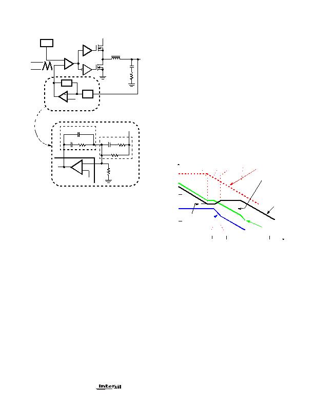
. The goal of the compensation network is to provide
a closed loop transfer function with high 0dB crossing
frequency (f
0dB
) and adequate phase margin. Phase margin
is the difference between the closed loop phase at f
0dB
and
180 degrees. The equations below relate the compensation
networks poles, zeros and gain to the components (R1 , R2 ,
R3 , C1 , C2 , and C3) in Figure 5. Use these guidelines for
locating the poles and zeros of the compensation network:
1. Pick Gain (R2/R1) for desired converter bandwidth
2. Place 1
ST
Zero Below Filters Double Pole (~75% F
LC
)
3. Place 2
ND
Zero at Filters Double Pole
4. Place 1
ST
Pole at the ESR Zero
5. Place 2
ND
Pole at Half the Switching Frequency
6. Check Gain against Error Amplifiers Open-Loop Gain
7. Estimate Phase Margin - Repeat if Necessary
Compensation Break Frequency Equations
Figure 6 shows an asymptotic plot of the DC-DC converters
gain vs. frequency. The actual Modulator Gain has a high
gain peak dependent on the quality factor (Q) of the output
filter, which is not shown in Figure 5. Using the above
guidelines should yield a Compensation Gain similar to the
curve plotted. The open loop error amplifier gain bounds the
compensation gain. Check the compensation gain at F
P2
with the capabilities of the error amplifier. The Closed Loop
Gain is constructed on the log-log graph of Figure 6 by
adding the Modulator Gain (in dB) to the Compensation Gain
(in dB). This is equivalent to multiplying the modulator
transfer function to the compensation transfer function and
plotting the gain.
The compensation gain uses external impedance networks
Z
FB
and Z
IN
to provide a stable, high bandwidth (BW) overall
loop. A stable control loop has a gain crossing with
-20dB/decade slope and a phase margin greater than 45
degrees. Include worst case component variations when
determining phase margin.
Individual Output Disable
The PWM and linear controllers can independently be
shutdown.
To disable the switching regulator, use an open-drain or
open-collector device capable of pulling the OCSET pin (with
the attached R
OCSET
pull-up) below 1.25V. To minimize the
possibility of OC trips at levels different than predicted, a
C
OCSET
capacitor with a value of an order of magnitude
larger than the output capacitance of the pull-down device,
has to be used in parallel with R
OCSET
(1nF recommended).
Upon turn-off of the pull-down device, the switching regulator
undergoes a soft-start cycle.
To disable a particular linear controller, pull and hold the
respective FB pin above a typical threshold of 1.25V. One
way to achieve this task is by using a logic gate coupled
FIGURE 5. VOLTAGE-MODE BUCK CONVERTER
COMPENSATION DESIGN
V
OUT
OSC
0.8V
L
O
C
O
ESR
V
IN
V
OSC
ERROR
AMP
PWM
DRIVER1
(PARASITIC)
Z
FB
+
-
0.8V
R
S1
R3
R2
C3
C2
C1
COMP
V
OUT
FB
Z
FB
ISL6521
Z
IN
COMP
DRIVER
DETAILED COMPENSATION COMPONENTS
PHASE
V
E/A
+
-
Z
IN
R
P1
SYNC
+
+
F
Z1
1
2?R
?2 C1
?/DIV>
-----------------------------------
=
F
Z2
1
2?nbsp R
S1
R3
+
(
) C3
?/DIV>
?/DIV>
----------------------------------------------------------
=
F
P1
1
2?R
2
C1 C2
?/DIV>
C1 C2
+
----------------------
?nbsp ?/DIV>
?nbsp ?/DIV>
?/DIV>
?/DIV>
-------------------------------------------------------
=
F
P2
1
2?R
?3 C3
?/DIV>
-----------------------------------
=
FIGURE 6. ASYMPTOTIC BODE PLOT OF CONVERTER GAIN
100
80
60
40
20
0
-20
-40
-60
F
P1
F
Z2
10M
1M
100K
10K
1K
100
10
OPEN LOOP
ERROR AMP GAIN
F
Z1
F
P2
F
LC
F
ESR
COMPENSATION
FREQUENCY (Hz)
GAIN
MODULATOR
GAIN
CLOSED LOOP
GAIN
20
V
IN
V
PP
------------
?nbsp ?/DIV>
?nbsp ?/DIV>
?nbsp ?/DIV>
log
20
R2
R
S1
-------------
?nbsp ?/DIV>
?nbsp ?/DIV>
?nbsp ?/DIV>
log
ISL6521
相关PDF资料 |
PDF描述 |
|---|---|
| RBC08DREN | CONN EDGECARD 16POS .100 EYELET |
| ISL6521CBZA-T | IC REG QD BCK/LINEAR 16-SOIC |
| RCC06DREI | CONN EDGECARD 12POS .100 EYELET |
| ABM40DTBD | CONN EDGECARD 80POS R/A .156 SLD |
| ABM40DTAN | CONN EDGECARD 80POS R/A .156 SLD |
相关代理商/技术参数 |
参数描述 |
|---|---|
| ISL6521EVAL1 | 功能描述:EVALUATION BOARD 1 ISL6521 RoHS:否 类别:编程器,开发系统 >> 过时/停产零件编号 系列:- 标准包装:1 系列:- 传感器类型:CMOS 成像,彩色(RGB) 传感范围:WVGA 接口:I²C 灵敏度:60 fps 电源电压:5.7 V ~ 6.3 V 嵌入式:否 已供物品:成像器板 已用 IC / 零件:KAC-00401 相关产品:4H2099-ND - SENSOR IMAGE WVGA COLOR 48-PQFP4H2094-ND - SENSOR IMAGE WVGA MONO 48-PQFP |
| ISL6521EVAL1Z | 功能描述:EVALUATION BOARD 1 ISL6521 RoHS:是 类别:编程器,开发系统 >> 评估板 - DC/DC 与 AC/DC(离线)SMPS 系列:- 产品培训模块:Obsolescence Mitigation Program 标准包装:1 系列:True Shutdown™ 主要目的:DC/DC,步升 输出及类型:1,非隔离 功率 - 输出:- 输出电压:- 电流 - 输出:1A 输入电压:2.5 V ~ 5.5 V 稳压器拓扑结构:升压 频率 - 开关:3MHz 板类型:完全填充 已供物品:板 已用 IC / 零件:MAX8969 |
| ISL6521IBZ | 功能描述:电压模式 PWM 控制器 4 IN 1 PWM/LINEAR CNTRLR 5V RoHS:否 制造商:Texas Instruments 输出端数量:1 拓扑结构:Buck 输出电压:34 V 输出电流: 开关频率: 工作电源电压:4.5 V to 5.5 V 电源电流:600 uA 最大工作温度:+ 125 C 最小工作温度:- 40 C 封装 / 箱体:WSON-8 封装:Reel |
| ISL6521IBZ-T | 功能描述:电压模式 PWM 控制器 4 IN 1 PWM/LINEAR CNTRLR 5V RoHS:否 制造商:Texas Instruments 输出端数量:1 拓扑结构:Buck 输出电压:34 V 输出电流: 开关频率: 工作电源电压:4.5 V to 5.5 V 电源电流:600 uA 最大工作温度:+ 125 C 最小工作温度:- 40 C 封装 / 箱体:WSON-8 封装:Reel |
| ISL6522ACB | 功能描述:IC REG CTRLR BST PWM VM 14-SOIC RoHS:否 类别:集成电路 (IC) >> PMIC - 稳压器 - DC DC 切换控制器 系列:- 标准包装:4,000 系列:- PWM 型:电压模式 输出数:1 频率 - 最大:1.5MHz 占空比:66.7% 电源电压:4.75 V ~ 5.25 V 降压:是 升压:无 回扫:无 反相:无 倍增器:无 除法器:无 Cuk:无 隔离:无 工作温度:-40°C ~ 85°C 封装/外壳:40-VFQFN 裸露焊盘 包装:带卷 (TR) |
发布紧急采购,3分钟左右您将得到回复。