- 您现在的位置:买卖IC网 > PDF目录15193 > ISL6522IVZ-T (Intersil)IC REG CTRLR BST PWM VM 14-TSSOP PDF资料下载
参数资料
| 型号: | ISL6522IVZ-T |
| 厂商: | Intersil |
| 文件页数: | 9/15页 |
| 文件大小: | 0K |
| 描述: | IC REG CTRLR BST PWM VM 14-TSSOP |
| 标准包装: | 2,500 |
| PWM 型: | 电压模式 |
| 输出数: | 1 |
| 频率 - 最大: | 1MHz |
| 占空比: | 100% |
| 电源电压: | 10.8 V ~ 13.2 V |
| 降压: | 是 |
| 升压: | 是 |
| 回扫: | 无 |
| 反相: | 无 |
| 倍增器: | 无 |
| 除法器: | 无 |
| Cuk: | 无 |
| 隔离: | 无 |
| 工作温度: | -40°C ~ 85°C |
| 封装/外壳: | 14-TSSOP(0.173",4.40mm 宽) |
| 包装: | 带卷 (TR) |
�� �
�
�ISL6522�
�OSC�
�DRIVER�
�V� IN�
�4.� Place� 1� ST� Pole� at� the� ESR� Zero�
�5.� Place� 2� ND� Pole� at� Half� the� Switching� Frequency�
�-�
�?� V� OSC�
�PWM�
�COMPARATOR�
�+�
�DRIVER�
�L� O�
�PHASE�
�C� O�
�V� OUT�
�6.� Check� Gain� against� Error� Amplifier� ’s� Open-Loop� Gain�
�7.� Estimate� Phase� Margin� -� Repeat� if� Necessary�
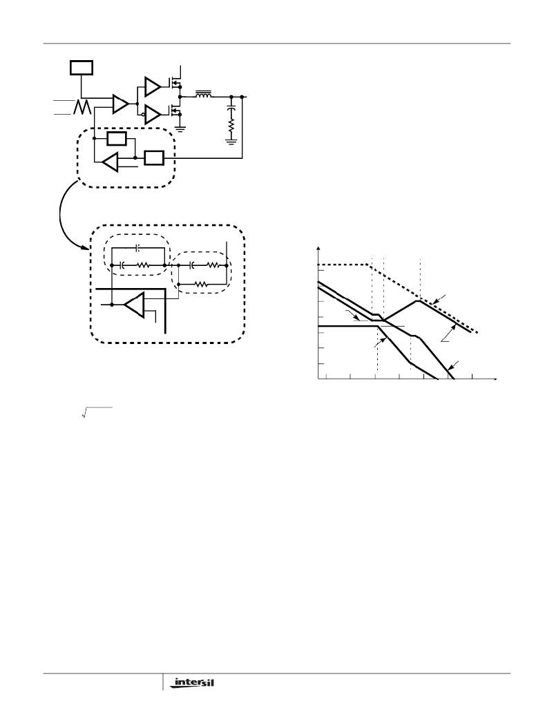
�Figure� 8� shows� an� asymptotic� plot� of� the� DC-DC� converter’s�
�-�
�Z� FB�
�V� E/A�
�+�
�ERROR�
�AMP�
�Z� IN�
�REFERENCE�
�ESR�
�(PARASITIC)�
�gain� vs.� frequency.� The� actual� modulator� gain� has� a� high� gain�
�peak� due� to� the� high� Q� factor� of� the� output� filter� and� is� not�
�shown� in� Figure� 8.� Using� the� above� guidelines� should� give� a�
�compensation� gain� similar� to� the� curve� plotted.� The� open� loop�
�error� amplifier� gain� bounds� the� compensation� gain.� Check� the�
�compensation� gain� at� F� P2� with� the� capabilities� of� the� error�
�amplifier.� The� closed� loop� gain� is� constructed� on� the� log-log�
�graph� of� Figure� 8� by� adding� the� modulator� gain� (in� dB)� to� the�
�DETAILED� COMPENSATION� COMPONENTS�
�compensation� gain� (in� dB).� This� is� equivalent� to� multiplying�
�the� modulator� transfer� function� to� the� compensation� transfer�
�C2�
�Z� FB�
�Z� IN�
�V� OUT�
�function� and� plotting� the� gain.�
�C1�
�COMP�
�-�
�+�
�R2�
�FB�
�C3�
�R3�
�R1�
�100�
�80�
�60�
�40�
�20LOG�
�F� Z1� F� Z2�
�F� P1�
�F� P2�
�OPEN� LOOP�
�ERROR� AMP� GAIN�
�ISL6522�
�REF�
�20�
�0�
�(R2/R1)�
�20LOG�
�(V� IN� /� ?� V� OSC� )�
�COMPENSATION�
�-20�
�MODULATOR�
�GAIN�
�FIGURE� 7.� VOLTAGE� -� MODE� BUCK� CONVERTER�
�COMPENSATION� DESIGN�
�Modulator� Break� Frequency� Equations�
�-40�
�-60�
�10�
�100�
�GAIN�
�1K�
�F� LC�
�10K�
�F� ESR�
�100K�
�1M�
�CLOSED� LOOP�
�GAIN�
�10M�
�F� LC� =� ---------------------------------------�
�F� ESR� =� ---------------------------------------------�
�1�
�2� π� ?� L� O� ?� C� O�
�1�
�2� π� ?� (� ESR� ?� C� O� )�
�FREQUENCY� (Hz)�
�FIGURE� 8.� ASYMPTOTIC� BODE� PLOT� OF� CONVERTER� GAIN�
�The� compensation� network� consists� of� the� error� amplifier�
�(internal� to� the� ISL6522)� and� the� impedance� networks� Z� IN�
�and� Z� FB� .� The� goal� of� the� compensation� network� is� to� provide�
�a� closed� loop� transfer� function� with� the� highest� 0dB� crossing�
�frequency� (f� 0dB� )� and� adequate� phase� margin.� Phase� margin�
�is� the� difference� between� the� closed� loop� phase� at� f� 0dB� and�
�180� degrees� .� The� equations� below� relate� the� compensation�
�network’s� poles,� zeros� and� gain� to� the� components� (R1,� R2,�
�R3,� C1,� C2,� and� C3)� in� Figure� 8.� Use� these� guidelines� for�
�locating� the� poles� and� zeros� of� the� compensation� network:�
�Compensation� Break� Frequency� Equations�
�The� compensation� gain� uses� external� impedance� networks�
�Z� FB� and� Z� IN� to� provide� a� stable,� high� bandwidth� (BW)� overall�
�loop.� A� stable� control� loop� has� a� gain� crossing� with�
�-20dB/decade� slope� and� a� phase� margin� greater� than� 45�
�degrees.� Include� worst� case� component� variations� when�
�determining� phase� margin.�
�Component� Selection� Guidelines�
�Output� Capacitor� Selection�
�An� output� capacitor� is� required� to� filter� the� output� and� supply�
�the� load� transient� current.� The� filtering� requirements� are� a�
�function� of� the� switching� frequency� and� the� ripple� current.�
�F� Z1� =� ----------------------------------�
�F� Z2� =� ------------------------------------------------------�
�F� P1� =� -------------------------------------------------------�
�2� π� ?� R2� ?� ?� ----------------------� ?�
�F� P2� =� ----------------------------------�
�1�
�2� π� ?� R� 2� ?� C1�
�1�
�2� π� ?� (� R1� +� R3� )� ?� C3�
�1�
�C1� ?� C2�
�?� C1� +� C2� ?�
�1�
�2� π� ?� R3� ?� C3�
�The� load� transient� requirements� are� a� function� of� the� slew�
�rate� (di/dt)� and� the� magnitude� of� the� transient� load� current.�
�These� requirements� are� generally� met� with� a� mix� of�
�capacitors� and� careful� layout.�
�Modern� microprocessors� produce� transient� load� rates� above�
�1.� Pick� Gain� (R2/R1)� for� desired� converter� bandwidth�
�2.� Place� 1� ST� Zero� Below� Filter� ’s� Double� Pole�
�(~75%� F� LC� )�
�3.� Place� 2� ND� Zero� at� Filter� ’s� Double� Pole�
�9�
�1A/ns.� High� frequency� capacitors� initially� supply� the� transient�
�and� slow� the� current� load� rate� seen� by� the� bulk� capacitors.�
�The� bulk� filter� capacitor� values� are� generally� determined� by�
�FN9030.8�
�March� 10,� 2006�
�相关PDF资料 |
PDF描述 |
|---|---|
| GCM43DCMH | CONN EDGECARD 86POS .156 WW |
| ISL88001IH23Z-T | IC VOLT SUPERVISOR 2.32V SOT23-3 |
| VE-JTM-EW-F2 | CONVERTER MOD DC/DC 10V 100W |
| ABC07DRYS-S734 | CONN EDGECARD 14POS DIP .100 SLD |
| ASC10DRTS-S734 | CONN EDGECARD 20POS DIP .100 SLD |
相关代理商/技术参数 |
参数描述 |
|---|---|
| ISL6522IVZ-TS2698 | 制造商:Intersil Corporation 功能描述:PB-FREE 14LD. TSSOP, T&R, PWM CONTROLLER- DRR REGUALTOR - Tape and Reel 制造商:Intersil Corporation 功能描述:IC REG CTRLR BUCK PWM 14TSSOP 制造商:Intersil 功能描述:14LD PWM CNTRLR- DRRGUALTOR |
| ISL6523ACB | 制造商:Rochester Electronics LLC 功能描述:- Bulk |
| ISL6523CB | 功能描述:IC CTRLR VRM8.5 PWM DUAL 28-SOIC RoHS:否 类别:集成电路 (IC) >> PMIC - 稳压器 - 专用型 系列:- 产品培训模块:Lead (SnPb) Finish for COTS Obsolescence Mitigation Program 标准包装:2,000 系列:- 应用:电源,ICERA E400,E450 输入电压:4.1 V ~ 5.5 V 输出数:10 输出电压:可编程 工作温度:-40°C ~ 85°C 安装类型:表面贴装 封装/外壳:42-WFBGA,WLCSP 供应商设备封装:42-WLP 包装:带卷 (TR) |
| ISL6523CB-T | 功能描述:IC CTRLR VRM8.5 PWM DUAL 28-SOIC RoHS:否 类别:集成电路 (IC) >> PMIC - 稳压器 - 专用型 系列:- 产品培训模块:Lead (SnPb) Finish for COTS Obsolescence Mitigation Program 标准包装:2,000 系列:- 应用:电源,ICERA E400,E450 输入电压:4.1 V ~ 5.5 V 输出数:10 输出电压:可编程 工作温度:-40°C ~ 85°C 安装类型:表面贴装 封装/外壳:42-WFBGA,WLCSP 供应商设备封装:42-WLP 包装:带卷 (TR) |
| ISL6523CBZ | 功能描述:IC CTRLR VRM8.5 PWM DUAL 28-SOIC RoHS:是 类别:集成电路 (IC) >> PMIC - 稳压器 - 专用型 系列:- 标准包装:43 系列:- 应用:控制器,Intel VR11 输入电压:5 V ~ 12 V 输出数:1 输出电压:0.5 V ~ 1.6 V 工作温度:-40°C ~ 85°C 安装类型:表面贴装 封装/外壳:48-VFQFN 裸露焊盘 供应商设备封装:48-QFN(7x7) 包装:管件 |
发布紧急采购,3分钟左右您将得到回复。