参数资料
| 型号: | ISL6548CRZA |
| 厂商: | Intersil |
| 文件页数: | 11/15页 |
| 文件大小: | 0K |
| 描述: | IC REG/CTRLR ACPI DUAL DDR 28QFN |
| 标准包装: | 50 |
| 应用: | 存储器,DDR/DDR2 稳压器 |
| 电流 - 电源: | 7mA |
| 工作温度: | 0°C ~ 70°C |
| 安装类型: | 表面贴装 |
| 封装/外壳: | 28-VQFN 裸露焊盘 |
| 供应商设备封装: | 28-QFN(6x6) |
| 包装: | 管件 |
�� �
�
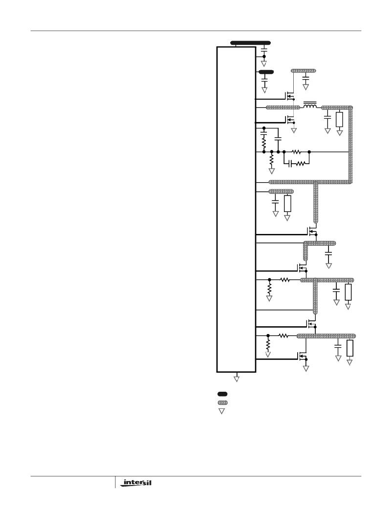
�ISL6548�
�critical� because� they� switch� large� amounts� of� energy,� and�
�therefore� tend� to� generate� large� amounts� of� noise.� Next� are�
�the� small� signal� components� which� connect� to� sensitive�
�nodes� or� supply� critical� bypass� current� and� signal� coupling.�
�12V� ATX�
�P12V�
�GNDP�
�C� BP�
�5VDUAL�
�A� multi-layer� printed� circuit� board� is� recommended.� Figure� 2�
�shows� the� connections� of� the� critical� components� in� the�
�5VSBY�
�5VSBY�
�C� BP�
�C� IN�
�converter.� Note� that� capacitors� C� IN� and� C� OUT� could� each�
�represent� numerous� physical� capacitors.� Dedicate� one� solid�
�layer,� usually� a� middle� layer� of� the� PC� board,� for� a� ground�
�ISL6548�
�UGATE�
�PHASE�
�Q� 1�
�L� 1�
�V� DDQ�
�plane� and� make� all� critical� component� ground� connections�
�with� vias� to� this� layer.� Dedicate� another� solid� layer� as� a�
�power� plane� and� break� this� plane� into� smaller� islands� of�
�LGATE�
�COMP�
�Q� 2�
�C� OUT1�
�common� voltage� levels.� Keep� the� metal� runs� from� the�
�PHASE� terminals� to� the� output� inductor� short.� The� power�
�plane� should� support� the� input� power� and� output� power�
�nodes.� Use� copper� filled� polygons� on� the� top� and� bottom�
�FB�
�C� 2�
�R� 2�
�R� 4�
�C� 1�
�R� 1�
�C� 3� R� 3�
�circuit� layers� for� the� phase� nodes.� Use� the� remaining� printed�
�circuit� layers� for� small� signal� wiring.� The� wiring� traces� from�
�the� GATE� pins� to� the� MOSFET� gates� should� be� kept� short�
�VDDQ(2)�
�V� DDQ�
�and� wide� enough� to� easily� handle� the� 1A� of� drive� current.�
�In� order� to� dissipate� heat� generated� by� the� internal� V� TT�
�LDO,� the� ground� pad,� pin� 29,� should� be� connected� to� the�
�internal� ground� plane� through� at� least� four� vias.� This� allows�
�the� heat� to� move� away� from� the� IC� and� also� ties� the� pad� to�
�the� ground� plane� through� a� low� impedance� path.�
�The� switching� components� should� be� placed� close� to� the�
�ISL6548� first.� Minimize� the� length� of� the� connections�
�VTT(2)�
�DRIVE4�
�FB4�
�C� OUT2�
�V� TT�
�Q� 3�
�between� the� input� capacitors,� C� IN� ,� and� the� power� switches�
�by� placing� them� nearby.� Position� both� the� ceramic� and� bulk�
�input� capacitors� as� close� to� the� upper� MOSFET� drain� as�
�DRIVE3�
�R� 5�
�Q� 4�
�C� OUT3�
�V� GMCH�
�possible.� Position� the� output� inductor� and� output� capacitors�
�FB3�
�between� the� upper� and� lower� MOSFETs� and� the� load.�
�The� critical� small� signal� components� include� any� bypass�
�capacitors,� feedback� components,� and� compensation�
�components.� Place� the� PWM� converter� compensation�
�REFADJ4�
�R� 6�
�C� OUT4�
�components� close� to� the� FB� and� COMP� pins.� The� feedback�
�resistors� should� be� located� as� close� as� possible� to� the� FB�
�pin� with� vias� tied� straight� to� the� ground� plane� as� required.�
�Feedback� Compensation� -� PWM� Buck� Converter�
�Figure� 3� highlights� the� voltage-mode� control� loop� for� a�
�DRIVE2_U�
�FB2�
�DRIVE2_L�
�R� 8�
�R� 7�
�Q� 6�
�Q� 5�
�V� TT_GMCH/CPU�
�C� OUT4�
�synchronous-rectified� buck� converter.� The� output� voltage�
�GND� PAD�
�(V� OUT� )� is� regulated� to� the� Reference� voltage� level.� The� error�
�amplifier� output� (V� E/A� )� is� compared� with� the� oscillator� (OSC)�
�triangular� wave� to� provide� a� pulse-width� modulated� (PWM)�
�wave� with� an� amplitude� of� V� IN� at� the� PHASE� node.� The�
�PWM� wave� is� smoothed� by� the� output� filter� (L� O� and� C� O� ).�
�The� modulator� transfer� function� is� the� small-signal� transfer�
�KEY�
�ISLAND� ON� POWER� PLANE� LAYER�
�ISLAND� ON� CIRCUIT� AND/OR� POWER� PLANE� LAYER�
�VIA� CONNECTION� TO� GROUND� PLANE�
�function� of� V� OUT� /V� E/A� .� This� function� is� dominated� by� a� DC�
�Gain� and� the� output� filter� (L� O� and� C� O� ),� with� a� double� pole�
�break� frequency� at� F� LC� and� a� zero� at� F� ESR� .� The� DC� Gain� of�
�the� modulator� is� simply� the� input� voltage� (V� IN� )� divided� by� the�
�peak-to-peak� oscillator� voltage� ?� V� OSC� .�
�11�
�FIGURE� 2.� PRINTED� CIRCUIT� BOARD� POWER� PLANES�
�AND� ISLANDS�
�FN9188.2�
�January� 3,� 2006�
�相关PDF资料 |
PDF描述 |
|---|---|
| ISL6551IR-T | IC REG CTRLR FLYBACK PWM 28-QFN |
| ISL6552CR-T | IC REG CTRLR BUCK PWM 20-QFN |
| ISL6553CB-T | IC REG CTRLR BUCK PWM 16-SOIC |
| ISL6554CB-T | IC PWM CORE VOLTAGE REG 20-SOIC |
| ISL6556ACR-T | IC CTRLR MULTIPHASE VRM10 32-QFN |
相关代理商/技术参数 |
参数描述 |
|---|---|
| ISL6548CRZA-T | 功能描述:电压模式 PWM 控制器 W/ANNEAL 4-IN-1G FOR DDR/I915/925 RoHS:否 制造商:Texas Instruments 输出端数量:1 拓扑结构:Buck 输出电压:34 V 输出电流: 开关频率: 工作电源电压:4.5 V to 5.5 V 电源电流:600 uA 最大工作温度:+ 125 C 最小工作温度:- 40 C 封装 / 箱体:WSON-8 封装:Reel |
| ISL6549CA | 功能描述:IC REG DL BCK/LINEAR 16-QSOP RoHS:否 类别:集成电路 (IC) >> PMIC - 稳压器 - 线性 + 切换式 系列:- 标准包装:2,500 系列:- 拓扑:降压(降压)同步(3),线性(LDO)(2) 功能:任何功能 输出数:5 频率 - 开关:300kHz 电压/电流 - 输出 1:控制器 电压/电流 - 输出 2:控制器 电压/电流 - 输出 3:控制器 带 LED 驱动器:无 带监控器:无 带序列发生器:是 电源电压:5.6 V ~ 24 V 工作温度:-40°C ~ 85°C 安装类型:* 封装/外壳:* 供应商设备封装:* 包装:* |
| ISL6549CA-T | 功能描述:IC REG DL BCK/LINEAR 16-QSOP RoHS:否 类别:集成电路 (IC) >> PMIC - 稳压器 - 线性 + 切换式 系列:- 标准包装:2,500 系列:- 拓扑:降压(降压)同步(3),线性(LDO)(2) 功能:任何功能 输出数:5 频率 - 开关:300kHz 电压/电流 - 输出 1:控制器 电压/电流 - 输出 2:控制器 电压/电流 - 输出 3:控制器 带 LED 驱动器:无 带监控器:无 带序列发生器:是 电源电压:5.6 V ~ 24 V 工作温度:-40°C ~ 85°C 安装类型:* 封装/外壳:* 供应商设备封装:* 包装:* |
| ISL6549CAZA | 功能描述:IC REG DL BCK/LINEAR 16-QSOP RoHS:是 类别:集成电路 (IC) >> PMIC - 稳压器 - 线性 + 切换式 系列:- 标准包装:2,500 系列:- 拓扑:降压(降压)同步(3),线性(LDO)(2) 功能:任何功能 输出数:5 频率 - 开关:300kHz 电压/电流 - 输出 1:控制器 电压/电流 - 输出 2:控制器 电压/电流 - 输出 3:控制器 带 LED 驱动器:无 带监控器:无 带序列发生器:是 电源电压:5.6 V ~ 24 V 工作温度:-40°C ~ 85°C 安装类型:* 封装/外壳:* 供应商设备封装:* 包装:* |
| ISL6549CAZAS2698 | 功能描述:IC REG DL BCK/LINEAR 16-QSOP RoHS:是 类别:集成电路 (IC) >> PMIC - 稳压器 - 线性 + 切换式 系列:- 标准包装:2,500 系列:- 拓扑:降压(降压)同步(3),线性(LDO)(2) 功能:任何功能 输出数:5 频率 - 开关:300kHz 电压/电流 - 输出 1:控制器 电压/电流 - 输出 2:控制器 电压/电流 - 输出 3:控制器 带 LED 驱动器:无 带监控器:无 带序列发生器:是 电源电压:5.6 V ~ 24 V 工作温度:-40°C ~ 85°C 安装类型:* 封装/外壳:* 供应商设备封装:* 包装:* |
发布紧急采购,3分钟左右您将得到回复。