- 您现在的位置:买卖IC网 > PDF目录15181 > ISL6567IRZ-T (Intersil)IC REG CTRLR BUCK PWM VM 24-QFN PDF资料下载
参数资料
| 型号: | ISL6567IRZ-T |
| 厂商: | Intersil |
| 文件页数: | 7/25页 |
| 文件大小: | 0K |
| 描述: | IC REG CTRLR BUCK PWM VM 24-QFN |
| 标准包装: | 6,000 |
| PWM 型: | 电压模式 |
| 输出数: | 1 |
| 频率 - 最大: | 1.5MHz |
| 占空比: | 66% |
| 电源电压: | 4.9 V ~ 5.5 V |
| 降压: | 是 |
| 升压: | 无 |
| 回扫: | 无 |
| 反相: | 无 |
| 倍增器: | 无 |
| 除法器: | 无 |
| Cuk: | 无 |
| 隔离: | 无 |
| 工作温度: | -40°C ~ 85°C |
| 封装/外壳: | 24-VFQFN 裸露焊盘 |
| 包装: | 带卷 (TR) |
�� �
�
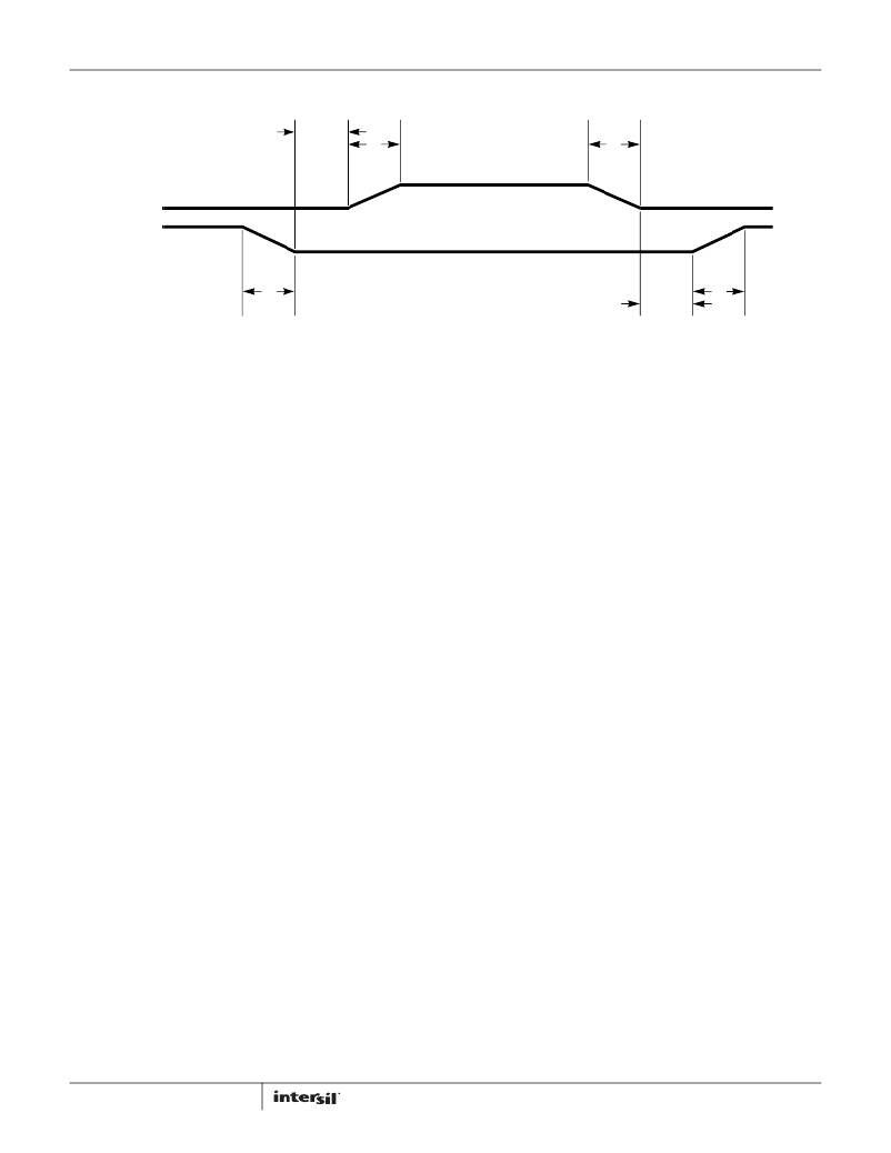
�ISL6567�
�Timing� Diagram�
�t� PDHUGATE�
�t� RUGATE�
�UGATE�
�LGATE�
�t� FLGATE�
�Functional� Pin� Description�
�VCC� (Pin� 8)�
�Bias� supply� for� the� IC’s� small-signal� circuitry.� Connect� this� pin�
�to� a� 5V� supply� and� locally� decouple� using� a� quality� 0.1μF�
�ceramic� capacitor.� This� pin� is� monitored� for� POR� purposes.� VCC�
�bias� may� be� applied� in� the� absence� of� PVCC� bias.�
�PVCC� (Pin� 15)�
�Power� supply� pin� for� the� MOSFET� drives.� Connect� this� pin� to� a�
�5V� supply� and� locally� decouple� using� a� quality� 1μF� ceramic�
�capacitor.� This� pin� is� monitored� for� POR� purposes.� PVCC� bias�
�should� not� be� applied� in� the� absence� of� VCC� bias.�
�VREG� (Pin� 7)�
�This� pin� is� the� output� of� the� internal� shunt� regulator.� The�
�internal� shunt� regulator� monitors� and� regulates� the� voltage� at�
�the� VCC� pin.� In� applications� where� the� chip� bias,� (including� that�
�necessary� to� drive� the� external� MOSFETs),� is� below� the� current�
�rating� of� this� pin,� connect� it� to� VCC� and� PVCC,� then� connect� this�
�node� to� the� input� supply� via� a� properly� sized� resistor.� Should�
�the� input� voltage� vary� over� a� wide� range� and/or� the� bias�
�current� required� exceed� the� intrinsic� capability� of� the� on-board�
�regulator,� use� this� pin� in� conjunction� with� an� external� NPN�
�transistor� and� a� couple� of� resistors� to� create� a� more� flexible�
�bias� supply� for� the� ISL6567.� In� any� configuration,� pay�
�particular� attention� to� the� chip’s� limitations� in� terms� of� both�
�current� sinking� capability� of� the� shunt� regulator,� as� well� as� the�
�internal� power� dissipation.�
�For� more� information,� refer� to� “Bias� Supply� Considerations”� on�
��GND� (Pin� 25)�
�Connect� this� pad� to� the� circuit� ground� using� the� shortest�
�possible� path� (one� to� four� vias� to� the� internal� ground� plane,�
�placed� on� the� soldering� pad� are� recommended).� All� internal�
�small-signal� circuitry,� as� well� as� the� lower� gates’� return� paths�
�are� referenced� to� this� pin.�
�REFTRK� (Pin� 24)�
�This� pin� represents� an� optional� reference� input,� as� well� as� a�
�clamp� voltage� for� the� internal� reference.� If� utilizing� the�
�ISL6567’s� internal� 0.6V� reference,� and� desire� no� special�
�7�
�t� FUGATE�
�t� RLGATE�
�t� PDHLGATE�
�tracking� features� enabled,� electrically� connect� this� pin� to� the�
�VCC� pin,� or� leave� it� open.� Internal� or� external� reference� operation�
�mode� is� dictated� by� the� MON� pin.�
�While� operating� in� internal� reference� mode,� this� pin� represents�
�an� internal� reference� clamp� that� can� be� used� for�
�implementation� of� various� tracking� features.� In� this� operating�
�mode,� a� small� internal� current� is� sourced� on� this� pin,� pulling� it�
�high� if� left� open.�
�If� utilizing� the� ISL6567� in� conjunction� with� an� external�
�reference,� connect� the� desired� stimulus� to� this� pin;� the� sensed�
�output� of� the� ISL6567� converter� follows� this� input.�
�While� operating� with� an� external� reference,� the� power-good� and�
�overvoltage� protection� functions� are� disabled� while� the� MON� pin�
�voltage� is� below� its� threshold� (typically� 300mV).�
�MON� (Pin� 3)�
�The� status� of� this� pin� is� checked� every� time� the� chip� is� enabled�
�or� POR� is� released;� should� its� potential� be� lower� than� 3.5V�
�(typical),� the� REFTRK� potential� is� assumed� to� be� an� externally-�
�provided� reference� and� the� ISL6567� proceeds� to� regulate� the�
�sensed� output� voltage� to� this� external� reference.� When�
�operating� using� the� internal� reference� voltage,� connect� this� pin�
�to� VCC� (to� bypass� the� mechanism� previously� described).�
�While� operating� with� an� externally-provided� reference,� connect�
�this� pin� to� a� properly-sized� resistor� divider� off� the� voltage� to� be�
�monitored.� PGOOD� and� OVP� functions� are� enabled� when� this�
�pin� exceeds� its� monitored� threshold� (typically� 300mV).�
�This� pin� is� normally� floating� (high� impedance� input)� until� it�
�exceeds� its� detect� threshold.� Once� the� threshold� is� exceeded,� a�
�small� current� is� sourced� on� this� pin;� this� current,� along� with� a�
�properly� sized� resistor� network,� allows� the� user� to� adjust� the�
�threshold� hysteresis.�
�For� more� information,� refer� to� “External� Reference� Operation”�
��EN� (Pin� 9)�
�This� pin� is� a� precision-threshold� (approximately� 0.6V)� enable� pin.�
�Pulled� above� the� threshold,� the� pin� enables� the� controller� for�
�operation,� initiating� a� soft-start.� Normally� a� high� impedance�
�input,� once� it� is� pulled� above� its� threshold,� a� small� current� is�
�sourced� on� this� pin;� this� current,� along� with� a� properly� sized�
�FN9243.4�
�August� 9,� 2011�
�相关PDF资料 |
PDF描述 |
|---|---|
| B41041A6158M | 1500UF 50V 16X35.5 SINGLE END |
| ISL6522IVZ | IC REG CTRLR BST PWM VM 14-TSSOP |
| ASC15DRTN | CONN EDGECARD 30POS .100 DIP SLD |
| H2ABT-10110-S4-ND | JUMPER-H1502TR/A2015S/H1500TR10" |
| H2ABT-10110-R4-ND | JUMPER-H1502TR/A2015R/H1500TR10" |
相关代理商/技术参数 |
参数描述 |
|---|---|
| ISL6567IRZ-TS2698 | 功能描述:IC REG CTRLR BUCK PWM VM 24-QFN RoHS:是 类别:集成电路 (IC) >> PMIC - 稳压器 - DC DC 切换控制器 系列:- 产品培训模块:Lead (SnPb) Finish for COTS Obsolescence Mitigation Program 标准包装:2,500 系列:- PWM 型:电流模式 输出数:1 频率 - 最大:275kHz 占空比:50% 电源电压:18 V ~ 110 V 降压:无 升压:无 回扫:无 反相:无 倍增器:无 除法器:无 Cuk:无 隔离:是 工作温度:-40°C ~ 85°C 封装/外壳:8-SOIC(0.154",3.90mm 宽) 包装:带卷 (TR) |
| ISL6568CR | 功能描述:IC CTRLR PWM BUCK 2PHASE 32-QFN RoHS:否 类别:集成电路 (IC) >> PMIC - 稳压器 - 专用型 系列:- 产品培训模块:Lead (SnPb) Finish for COTS Obsolescence Mitigation Program 标准包装:2,000 系列:- 应用:电源,ICERA E400,E450 输入电压:4.1 V ~ 5.5 V 输出数:10 输出电压:可编程 工作温度:-40°C ~ 85°C 安装类型:表面贴装 封装/外壳:42-WFBGA,WLCSP 供应商设备封装:42-WLP 包装:带卷 (TR) |
| ISL6568CR-T | 功能描述:IC CTRLR PWM BUCK 2PHASE 32-QFN RoHS:否 类别:集成电路 (IC) >> PMIC - 稳压器 - 专用型 系列:- 产品培训模块:Lead (SnPb) Finish for COTS Obsolescence Mitigation Program 标准包装:2,000 系列:- 应用:电源,ICERA E400,E450 输入电压:4.1 V ~ 5.5 V 输出数:10 输出电压:可编程 工作温度:-40°C ~ 85°C 安装类型:表面贴装 封装/外壳:42-WFBGA,WLCSP 供应商设备封装:42-WLP 包装:带卷 (TR) |
| ISL6568CRZ | 制造商:Intersil Corporation 功能描述:CURRENT MODE PWM CNTRLR 0.8375V TO 12V 60A 32QFN EP - Rail/Tube 制造商:Intersil 功能描述:2-PH PWM CNTRLR VRM9 W/2-DRVRS 10 K8 DAC |
| ISL6568CRZA | 制造商:Intersil Corporation 功能描述:CURRENT MODE PWM CNTRLR 0.8375V TO 12V 60A 32QFN EP - Rail/Tube 制造商:Intersil 功能描述:W/ANNEAL 2-PH PWM CNTRLR 2-DRVRS VRM9 |
发布紧急采购,3分钟左右您将得到回复。