- 您现在的位置:买卖IC网 > PDF目录20574 > ISL6596IRZ (Intersil)IC MOSFET DRVR SYNC BUCK 10-DFN PDF资料下载
参数资料
| 型号: | ISL6596IRZ |
| 厂商: | Intersil |
| 文件页数: | 9/11页 |
| 文件大小: | 0K |
| 描述: | IC MOSFET DRVR SYNC BUCK 10-DFN |
| 标准包装: | 100 |
| 配置: | 高端和低端,同步 |
| 输入类型: | PWM |
| 延迟时间: | 19ns |
| 电流 - 峰: | 2A |
| 配置数: | 1 |
| 输出数: | 2 |
| 高端电压 - 最大(自引导启动): | 36V |
| 电源电压: | 4.5 V ~ 5.5 V |
| 工作温度: | -40°C ~ 85°C |
| 安装类型: | 表面贴装 |
| 封装/外壳: | 10-VFDFN 裸露焊盘 |
| 供应商设备封装: | 10-DFN-EP(3x3) |
| 包装: | 管件 |
�� �
�
�ISL6596�
�Application� Information�
�MOSFET� Selection�
�The� parasitic� inductances� of� the� PCB� and� of� the� power�
�devices’� packaging� (both� upper� and� lower� MOSFETs)� can�
�cause� serious� ringing,� exceeding� absolute� maximum� rating�
�of� the� devices.� The� negative� ringing� at� the� edges� of� the�
�PHASE� node� could� increase� the� bootstrap� capacitor� voltage�
�through� the� internal� bootstrap� diode,� and� in� some� cases,� it�
�may� overstress� the� upper� MOSFET� driver.� Careful� layout,�
�proper� selection� of� MOSFETs� and� packaging� can� go� a� long�
�way� toward� minimizing� such� unwanted� stress.�
�The� D� 2� -PAK,� or� D-PAK� packaged� MOSFETs,� have� large�
�parasitic� lead� inductances� and� are� not� recommended� unless�
�additional� circuits� are� implemented� to� prevent� the� BOOT� and�
�PHASE� pins� from� exceeding� the� device� rating.� Low-profile�
�MOSFETs,� such� as� Direct� FETs� and� multi-SOURCE� leads�
�devices� (SO-8,� LFPAK,� PowerPAK),� have� low� parasitic� lead�
�inductances� and� are� preferred.�
�Layout� Considerations�
�A� good� layout� helps� reduce� the� ringing� on� the� switching�
�node� (PHASE)� and� significantly� lowers� the� stress� applied� to�
�the� output� drives.� The� following� advice� is� meant� to� lead� to� an�
�optimized� layout:�
�?� Keep� decoupling� loops� (VCC-GND� and� BOOT-PHASE)� as�
�short� as� possible.�
�?� Minimize� trace� inductance,� especially� on� low-impedance�
�lines.� All� power� traces� (UGATE,� PHASE,� LGATE,� GND,�
�VCC)� should� be� short� and� wide,� as� much� as� possible.�
�?� Minimize� the� inductance� of� the� PHASE� node.� Ideally,� the�
�Upper� MOSFET� Self� Turn-On� Effects� At� Startup�
�Should� the� driver� have� insufficient� bias� voltage� applied,� its�
�outputs� are� floating.� If� the� input� bus� is� energized� at� a� high�
�dV/dt� rate� while� the� driver� outputs� are� floating,� because� of�
�self-coupling� via� the� internal� C� GD� of� the� MOSFET,� the�
�UGATE� could� momentarily� rise� up� to� a� level� greater� than� the�
�threshold� voltage� of� the� MOSFET.� This� could� potentially� turn�
�on� the� upper� switch� and� result� in� damaging� inrush� energy.�
�Therefore,� if� such� a� situation� (when� input� bus� powered� up�
�before� the� bias� of� the� controller� and� driver� is� ready)� could�
�conceivably� be� encountered,� it� is� a� common� practice� to�
�place� a� resistor� (R� UGPH� )� across� the� gate� and� source� of� the�
�upper� MOSFET� to� suppress� the� Miller� coupling� effect.� The�
�value� of� the� resistor� depends� mainly� on� the� input� voltage’s�
�rate� of� rise,� the� C� GD� /C� GS� ratio,� as� well� as� the� gate-source�
�threshold� of� the� upper� MOSFET.� A� higher� dV/dt,� a� lower�
�C� DS� /C� GS� ratio,� and� a� lower� gate-source� threshold� upper�
�FET� will� require� a� smaller� resistor� to� diminish� the� effect� of�
�the� internal� capacitive� coupling.� For� most� applications,� a�
�5k� Ω� to� 10k� Ω� resistor� is� typically� sufficient,� not� affecting�
�normal� performance� and� efficiency.�
�The� coupling� effect� can� be� roughly� estimated� with� the�
�following� equations,� which� assume� a� fixed� linear� input� ramp�
�and� neglect� the� clamping� effect� of� the� body� diode� of� the�
�upper� drive� and� the� bootstrap� capacitor.� Other� parasitic�
�components� such� as� lead� inductances� and� PCB�
�capacitances� are� also� not� taken� into� account.� These�
�equations� are� provided� for� guidance� purpose� only.�
�Therefore,� the� actual� coupling� effect� should� be� examined�
�using� a� very� high� impedance� (10M� Ω� or� greater)� probe� to�
�ensure� a� safe� design� margin.�
�–� V�
�?�
�----------------------------------� ?�
�?� dV� ?�
�V� GS_MILLER� =� -------� ?� R� ?� C� rss� ?� 1� –� e� dt�
�iss� ?�
�-------� ?� R� ?� C�
�source� of� the� upper� and� the� drain� of� the� lower� MOSFET�
�should� be� as� close� as� thermally� allowable.�
�?� Minimize� the� current� loop� of� the� output� and� input� power�
�trains.� Short� the� source� connection� of� the� lower� MOSFET�
�to� ground� as� close� to� the� transistor� pin� as� feasible.� Input�
�dV�
�DS�
�dt� ?� ?�
�?� ?�
�?� ?�
�(EQ.� 5)�
�capacitors� (especially� ceramic� decoupling)� should� be�
�placed� as� close� to� the� drain� of� upper� and� source� of� lower�
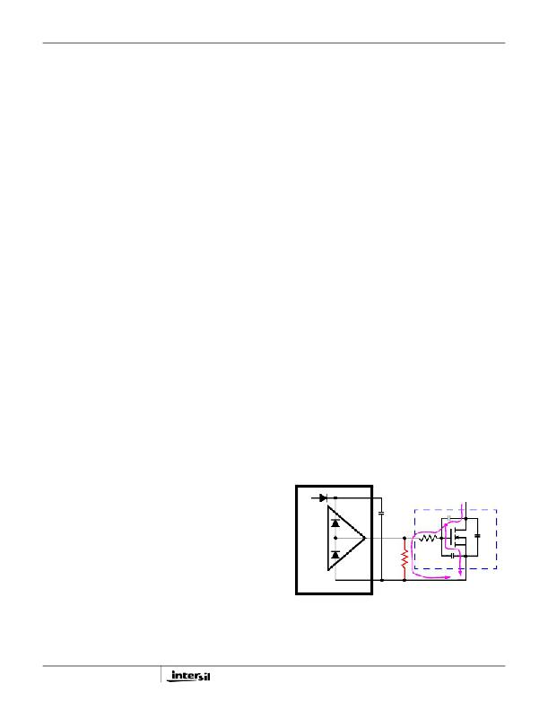
�R� =� R� UGPH� +� R� GI�
�C� rss� =� C� GD�
�C� iss� =� C� GD� +� C� GS�
�MOSFETs� as� possible.�
�In� addition,� for� heat� spreading,� place� copper� underneath� the�
�VCC�
�BOOT�
�VIN�
�IC� whether� it� has� an� exposed� pad� or� not.� The� copper� area�
�can� be� extended� beyond� the� bottom� area� of� the� IC� and/or�
�connected� to� buried� power� ground� plane(s)� with� thermal�
�C� BOOT�
�C� GD�
�D�
�vias.� This� combination� of� vias� for� vertical� heat� escape,�
�extended� copper� plane,� and� buried� planes� improve� heat�
�dissipation� and� allow� the� part� to� achieve� its� full� thermal�
�potential� .�
�DU�
�DL�
�UGATE�
�G�
�R� GI�
�C� GS�
�C� DS�
�Q� UPPER�
�S�
�PHASE�
�FIGURE� 5.� GATE� TO� SOURCE� RESISTOR� TO� REDUCE�
�UPPER� MOSFET� MILLER� COUPLING�
�9�
�FN9240.1�
�January� 22,� 2010�
�相关PDF资料 |
PDF描述 |
|---|---|
| ASPI-2510-1R0N-T2 | INDUCTOR CHIP 1.0UH 2510 SMD |
| F951A476MBAAQ2 | CAP TANT 47UF 10V 20% 1210 |
| T95S105M025LSAL | CAP TANT 1UF 25V 20% 1507 |
| ECC12DCST | CONN EDGECARD 24POS DIP .100 SLD |
| VI-B03-CY-B1 | CONVERTER MOD DC/DC 24V 50W |
相关代理商/技术参数 |
参数描述 |
|---|---|
| ISL6596IRZ-T | 功能描述:IC MOSFET DRVR SYNC BUCK 10-DFN RoHS:是 类别:集成电路 (IC) >> PMIC - MOSFET,电桥驱动器 - 外部开关 系列:- 标准包装:50 系列:- 配置:高端 输入类型:非反相 延迟时间:200ns 电流 - 峰:250mA 配置数:1 输出数:1 高端电压 - 最大(自引导启动):600V 电源电压:12 V ~ 20 V 工作温度:-40°C ~ 125°C 安装类型:通孔 封装/外壳:8-DIP(0.300",7.62mm) 供应商设备封装:8-DIP 包装:管件 其它名称:*IR2127 |
| ISL6597CRZ | 功能描述:IC MOSFET DRVR DUAL SYNC 16-QFN RoHS:是 类别:集成电路 (IC) >> PMIC - MOSFET,电桥驱动器 - 外部开关 系列:- 标准包装:50 系列:- 配置:高端 输入类型:非反相 延迟时间:200ns 电流 - 峰:250mA 配置数:1 输出数:1 高端电压 - 最大(自引导启动):600V 电源电压:12 V ~ 20 V 工作温度:-40°C ~ 125°C 安装类型:通孔 封装/外壳:8-DIP(0.300",7.62mm) 供应商设备封装:8-DIP 包装:管件 其它名称:*IR2127 |
| ISL6597CRZ-T | 功能描述:IC MOSFET DRVR DUAL SYNC 16-QFN RoHS:是 类别:集成电路 (IC) >> PMIC - MOSFET,电桥驱动器 - 外部开关 系列:- 标准包装:50 系列:- 配置:高端 输入类型:非反相 延迟时间:200ns 电流 - 峰:250mA 配置数:1 输出数:1 高端电压 - 最大(自引导启动):600V 电源电压:12 V ~ 20 V 工作温度:-40°C ~ 125°C 安装类型:通孔 封装/外壳:8-DIP(0.300",7.62mm) 供应商设备封装:8-DIP 包装:管件 其它名称:*IR2127 |
| ISL6598DRZ-T | 制造商:Intersil Corporation 功能描述:PB-FREE 48LD 7X7 QFN, T&R, GRAPHICS PROCESSOR DIGITAL CONT. - Tape and Reel 制造商:Intersil Corporation 功能描述:IC GRAPHICS PROCESSOR DGTL 制造商:Intersil 功能描述:4 8LD 7X7 GRAPHICS PROCESSOR DIGTL CONT |
| ISL6605CB | 功能描述:IC MOSFET DRVR SYNC BUCK 8-SOIC RoHS:否 类别:集成电路 (IC) >> PMIC - MOSFET,电桥驱动器 - 外部开关 系列:- 标准包装:50 系列:- 配置:低端 输入类型:非反相 延迟时间:40ns 电流 - 峰:9A 配置数:1 输出数:1 高端电压 - 最大(自引导启动):- 电源电压:4.5 V ~ 35 V 工作温度:-40°C ~ 125°C 安装类型:表面贴装 封装/外壳:TO-263-6,D²Pak(5 引线+接片),TO-263BA 供应商设备封装:TO-263 包装:管件 |
发布紧急采购,3分钟左右您将得到回复。