- 您现在的位置:买卖IC网 > PDF目录20378 > ISL6608CB-T (Intersil)IC MOSFET DRVR SYNC BUCK 8-SOIC PDF资料下载
参数资料
| 型号: | ISL6608CB-T |
| 厂商: | Intersil |
| 文件页数: | 8/11页 |
| 文件大小: | 0K |
| 描述: | IC MOSFET DRVR SYNC BUCK 8-SOIC |
| 标准包装: | 2,500 |
| 配置: | 高端和低端,同步 |
| 输入类型: | PWM |
| 延迟时间: | 20ns |
| 电流 - 峰: | 2A |
| 配置数: | 1 |
| 输出数: | 2 |
| 电源电压: | 4.5 V ~ 5.5 V |
| 工作温度: | 0°C ~ 70°C |
| 安装类型: | 表面贴装 |
| 封装/外壳: | 8-SOIC(0.154",3.90mm 宽) |
| 供应商设备封装: | 8-SOIC |
| 包装: | 带卷 (TR) |
�� �
�
�ISL6608�
�C� BOOT� ≥� ------------------------�
�Q� G1� ?� VCC�
�Q� GATE� =� -------------------------------� ?� N� Q1�
�Diode� Emulation�
�Diode� emulation� allows� for� higher� converter� efficiency� under�
�light-load� situations.� With� diode� emulation� active�
�(FCCM� =� LO),� the� ISL6608� will� detect� the� zero� current�
�crossing� of� the� output� inductor� and� turn� off� LGATE.� This�
�ensures� that� discontinuous� conduction� mode� (DCM)� is�
�achieved.� This� prevents� the� low� side� MOSFET� from� sinking�
�current,� and� no� negative� spike� at� the� output� is� generated�
�during� pre-biased� startup� (See� Figure� 7� on� page� 7).� The�
�LGATE� has� a� minimum� ON� time� of� 400ns� in� DCM� mode.�
�Diode� emulation� is� asynchronous� to� the� PWM� signal.�
�Therefore,� the� ISL6608� responds� to� the� FCCM� input�
�immediately� after� it� changes� state.� Refer� to� Figures� 2� to� 7� on�
�page� 7� for� details.�
�Intersil� does� not� recommend� Diode� Emulation� used� with� the�
�r� DS(ON)� of� the� freewheeling� MOSFET� current� sensing�
�topology.� The� turn-OFF� of� the� low� side� MOSFET� forces� the�
�forward� current� going� through� the� body� diode� of� the�
�MOSFET.� If� the� current� sampling� circuit� of� the� controller� is�
�activated� during� the� body� diode� conduction,� a� diode� voltage�
�drop,� instead� of� a� much� smaller� MOSFET’s� r� DS(ON)� voltage�
�drop,� is� sampled.� This� will� falsely� trigger� the� over� current�
�protection� function� of� the� controller.�
�The� ISL6608� works� with� DCR,� upper� MOSFET,� or� power�
�resistor� current� sensing� topologies� to� start� up� from� pre-�
�biased� load� with� no� problem.�
�Three-State� PWM� Input�
�A� unique� feature� of� the� ISL6608� and� other� Intersil� drivers� is�
�the� addition� of� a� shutdown� window� to� the� PWM� input.� If� the�
�PWM� signal� enters� and� remains� within� the� shutdown� window�
�for� a� set� holdoff� time� (typically� 160ns),� the� output� drivers� are�
�disabled� and� both� MOSFET� gates� are� pulled� and� held� low.�
�The� shutdown� state� is� removed� when� the� PWM� signal�
�moves� outside� the� shutdown� window.� Otherwise,� the� PWM�
�rising� and� falling� thresholds� outlined� in� the� ELECTRICAL�
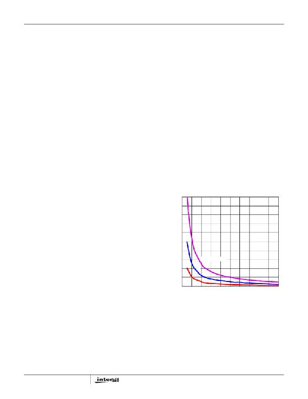
�Internal� Bootstrap� Diode�
�This� driver� features� an� internal� bootstrap� Schottky� diode.�
�Simply� adding� an� external� capacitor� across� the� BOOT� and�
�PHASE� pins� completes� the� bootstrap� circuit.� The� bootstrap�
�capacitor� must� have� a� maximum� voltage� rating� above� VCC� +�
�5V� and� its� capacitance� value� can� be� chosen� from� the�
�following� equation:�
�Q� GATE�
�?� V� BOOT�
�V� GS1�
�where� Q� G1� is� the� amount� of� gate� charge� per� upper� MOSFET�
�at� V� GS1� gate-source� voltage� and� N� Q1� is� the� number� of�
�control� MOSFETs.� The� ?� V� BOOT� term� is� defined� as� the�
�allowable� droop� in� the� rail� of� the� upper� drive.� The� previous�
�relationship� is� illustrated� in� Figure� 8.�
�As� an� example,� suppose� an� upper� MOSFET� has� a� gate�
�charge,� Q� GATE� ,� of� 65nC� at� 5V� and� also� assume� the� droop� in�
�the� drive� voltage� over� a� PWM� cycle� is� 200mV.� One� will� find�
�that� a� bootstrap� capacitance� of� at� least� 0.125� μ� F� is� required.�
�The� next� larger� standard� value� capacitance� is� 0.15� μ� F.� A�
�good� quality� ceramic� capacitor� is� recommended.�
�2.0�
�1.8�
�1.6�
�1.4�
�1.2�
�1.0�
�0.8�
�SPECIFICATIONS� determine� when� the� lower� and� upper�
�gates� are� enabled.�
�Adaptive� Shoot-Through� Protection�
�Both� drivers� incorporate� adaptive� shoot-through� protection�
�0.6�
�0.4�
�0.2�
�20nC�
�Q� GATE� = 100nC�
�to� prevent� upper� and� lower� MOSFETs� from� conducting�
�simultaneously� and� shorting� the� input� supply.� This� is�
�0.0�
�0.0�
�0.1�
�0.2�
�0.3�
�0.4�
�0.5�
�0.6�
�0.7�
�0.8�
�0.9�
�1.0�
�accomplished� by� ensuring� the� falling� gate� has� turned� off� one�
�MOSFET� before� the� other� is� allowed� to� turn� on.�
�During� turn-off� of� the� lower� MOSFET,� the� LGATE� voltage� is�
�monitored� until� it� reaches� a� 1V� threshold,� at� which� time� the�
�UGATE� is� released� to� rise.� Adaptive� shoot-through� circuitry�
�monitors� the� upper� MOSFET� gate-to-source� voltage� during�
�UGATE� turn-off.� Once� the� upper� MOSFET� gate-to-source�
�voltage� has� dropped� below� a� threshold� of� 1V,� the� LGATE� is�
�allowed� to� rise.�
�8�
�?� V� BOOT_CAP� (V)�
�FIGURE� 8.� BOOTSTRAP� CAPACITANCE� vs� BOOT� RIPPLE�
�VOLTAGE�
�相关PDF资料 |
PDF描述 |
|---|---|
| VE-BNF-CW-F3 | CONVERTER MOD DC/DC 72V 100W |
| VE-BNF-CW-F2 | CONVERTER MOD DC/DC 72V 100W |
| VE-BNF-CW-F1 | CONVERTER MOD DC/DC 72V 100W |
| VE-BND-CX-F4 | CONVERTER MOD DC/DC 85V 75W |
| F720J157KRC | CAP TANT 150UF 6.3V 10% 2824 |
相关代理商/技术参数 |
参数描述 |
|---|---|
| ISL6608CBZ | 功能描述:功率驱动器IC VER OF ISL6608CB RoHS:否 制造商:Micrel 产品:MOSFET Gate Drivers 类型:Low Cost High or Low Side MOSFET Driver 上升时间: 下降时间: 电源电压-最大:30 V 电源电压-最小:2.75 V 电源电流: 最大功率耗散: 最大工作温度:+ 85 C 安装风格:SMD/SMT 封装 / 箱体:SOIC-8 封装:Tube |
| ISL6608CBZ-T | 功能描述:功率驱动器IC VER OF ISL6608CB-T RoHS:否 制造商:Micrel 产品:MOSFET Gate Drivers 类型:Low Cost High or Low Side MOSFET Driver 上升时间: 下降时间: 电源电压-最大:30 V 电源电压-最小:2.75 V 电源电流: 最大功率耗散: 最大工作温度:+ 85 C 安装风格:SMD/SMT 封装 / 箱体:SOIC-8 封装:Tube |
| ISL6608CR | 功能描述:IC MOSFET DRVR SYNC BUCK 8-QFN RoHS:否 类别:集成电路 (IC) >> PMIC - MOSFET,电桥驱动器 - 外部开关 系列:- 标准包装:50 系列:- 配置:低端 输入类型:非反相 延迟时间:40ns 电流 - 峰:9A 配置数:1 输出数:1 高端电压 - 最大(自引导启动):- 电源电压:4.5 V ~ 35 V 工作温度:-40°C ~ 125°C 安装类型:表面贴装 封装/外壳:TO-263-6,D²Pak(5 引线+接片),TO-263BA 供应商设备封装:TO-263 包装:管件 |
| ISL6608CR-T | 功能描述:IC MOSFET DRVR SYNC BUCK 8-QFN RoHS:否 类别:集成电路 (IC) >> PMIC - MOSFET,电桥驱动器 - 外部开关 系列:- 标准包装:50 系列:- 配置:低端 输入类型:非反相 延迟时间:40ns 电流 - 峰:9A 配置数:1 输出数:1 高端电压 - 最大(自引导启动):- 电源电压:4.5 V ~ 35 V 工作温度:-40°C ~ 125°C 安装类型:表面贴装 封装/外壳:TO-263-6,D²Pak(5 引线+接片),TO-263BA 供应商设备封装:TO-263 包装:管件 |
| ISL6608CRZ | 功能描述:功率驱动器IC VER OF ISL6608CR RoHS:否 制造商:Micrel 产品:MOSFET Gate Drivers 类型:Low Cost High or Low Side MOSFET Driver 上升时间: 下降时间: 电源电压-最大:30 V 电源电压-最小:2.75 V 电源电流: 最大功率耗散: 最大工作温度:+ 85 C 安装风格:SMD/SMT 封装 / 箱体:SOIC-8 封装:Tube |
发布紧急采购,3分钟左右您将得到回复。