- 您现在的位置:买卖IC网 > Datasheet目录334 > ISL6614CRZ (Intersil)IC DRIVER MOSF DUAL SYNC 16QFN Datasheet资料下载
参数资料
| 型号: | ISL6614CRZ |
| 厂商: | Intersil |
| 文件页数: | 10/12页 |
| 文件大小: | 0K |
| 描述: | IC DRIVER MOSF DUAL SYNC 16QFN |
| 标准包装: | 75 |
| 配置: | 高端和低端,同步 |
| 输入类型: | PWM |
| 延迟时间: | 10ns |
| 电流 - 峰: | 1.25A |
| 配置数: | 2 |
| 输出数: | 4 |
| 高端电压 - 最大(自引导启动): | 36V |
| 电源电压: | 10.8 V ~ 13.2 V |
| 工作温度: | 0°C ~ 85°C |
| 安装类型: | 表面贴装 |
| 封装/外壳: | 16-VQFN 裸露焊盘 |
| 供应商设备封装: | 16-QFN-EP(4x4) |
| 包装: | 管件 |
| 产品目录页面: | 1241 (CN2011-ZH PDF) |
�� �
�
�ISL6614�
�the� SO14� package� is� approximately� 1W� at� room�
�temperature,� while� the� power� dissipation� capacity� in� the�
�QFN� packages,� with� an� exposed� heat� escape� pad,� is� around�
�2W.� See� “Layout� Considerations”� on� page� 10� for� thermal�
�PVCC�
�BOOT�
�C� GD�
�D�
�transfer� improvement� suggestions.� When� designing� the�
�driver� into� an� application,� it� is� recommended� that� the�
�following� calculation� is� used� to� ensure� safe� operation� at� the�
�desired� frequency� for� the� selected� MOSFETs.� The� total� gate�
�R� HI1�
�R� LO1�
�G�
�R� G1�
�R� GI1�
�C� GS�
�C� DS�
�Q1�
�drive� power� losses� due� to� the� gate� charge� of� MOSFETs� and�
�the� driver� ’s� internal� circuitry� and� their� corresponding� average�
�driver� current� can� be� estimated� using� Equations� 2� and� 3,�
�PHASE�
�S�
�respectively:�
�P� Qg_TOT� =� 2� ?� P� Qg_Q1� +� 2� ?� P� Qg_Q2� +� I� Q� ?� VCC�
�(EQ.� 2)�
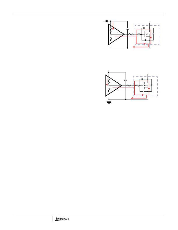
�FIGURE� 3.� TYPICAL� UPPER-GATE� DRIVE� TURN-ON� PATH�
�P� Qg_Q1� =� ---------------------------------------� ?� F� SW� ?� N� Q1�
�Q� G1� ?� PVCC� 2�
�V� GS1�
�PVCC�
�D�
�Q� G2�
�P� Qg_Q2� =� ---------------------------------------� ?� F� SW� ?� N� Q2�
�I� DR� =� ?� ------------------------------� +� ------------------------------� ?� ?� F� SW� ?� 2� +� I� Q�
�?� PVCC� 2�
�V� GS2�
�?� Q� G1� ?� N� Q1� Q� G2� ?� N� Q2� ?�
�?� V� GS1� V� GS2� ?�
�R� HI2�
�R� LO2�
�G�
�R� G2�
�C� GD�
�R� GI2�
�C� GS�
�S�
�C� DS�
�Q2�
�(EQ.� 3)�
�where� the� gate� charge� (Q� G1� and� Q� G2� )� is� defined� at� a�
�particular� gate� to� source� voltage� (V� GS1� and� V� GS2� )� in� the�
�corresponding� MOSFET� datasheet;� I� Q� is� the� driver� ’s� total�
�quiescent� current� with� no� load� at� both� drive� outputs;� N� Q1�
�and� N� Q2� are� number� of� upper� and� lower� MOSFETs,�
�respectively;� PVCC� is� the� drive� voltages� for� both� upper� and�
�lower� FETs,� respectively.� The� I� Q*� VCC� product� is� the�
�quiescent� power� of� the� driver� without� capacitive� load� and� is�
�typically� 200mW� at� 300kHz.�
�The� total� gate� drive� power� losses� are� dissipated� among� the�
�resistive� components� along� the� transition� path.� The� drive�
�resistance� dissipates� a� portion� of� the� total� gate� drive� power�
�losses,� the� rest� will� be� dissipated� by� the� external� gate�
�resistors� (R� G1� and� R� G2� )� and� the� internal� gate� resistors�
�(R� GI1� and� R� GI2� )� of� MOSFETs.� Figures� 3� and� 4� show� the�
�typical� upper� and� lower� gate� drives� turn-on� transition� path.�
�The� power� dissipation� on� the� driver� can� be� roughly�
�estimated� as:�
�FIGURE� 4.� TYPICAL� LOWER-GATE� DRIVE� TURN-ON� PATH�
�Layout� Considerations�
�For� heat� spreading,� place� copper� underneath� the� IC� whether�
�it� has� an� exposed� pad� or� not.� The� copper� area� can� be�
�extended� beyond� the� bottom� area� of� the� IC� and/or�
�connected� to� buried� copper� plane(s)� with� thermal� vias.� This�
�combination� of� vias� for� vertical� heat� escape,� extended�
�copper� plane,� and� buried� planes� for� heat� spreading� allows�
�the� IC� to� achieve� its� full� thermal� potential.�
�Place� each� channel� power� component� as� close� to� each�
�other� as� possible� to� reduce� PCB� copper� losses� and� PCB�
�parasitics:� shortest� distance� between� DRAINs� of� upper� FETs�
�and� SOURCEs� of� lower� FETs;� shortest� distance� between�
�DRAINs� of� lower� FETs� and� the� power� ground.� Thus,� smaller�
�amplitudes� of� positive� and� negative� ringing� are� on� the�
�switching� edges� of� the� PHASE� node.� However,� some� space�
�in� between� the� power� components� is� required� for� good�
�P� DR_UP� =� ?� --------------------------------------� +� ----------------------------------------� ?� ?� ---------------------�
�?� R� HI1� +� R� EXT1� R� LO1� +� R� EXT1� ?�
�P� DR_LOW� =� ?� --------------------------------------� +� ----------------------------------------� ?� ?� ---------------------�
�?� R� HI2� +� R� EXT2� R� LO2� +� R� EXT2� ?�
�R� EXT1� =� R� G1� +� -------------�
�N�
�R� EXT2� =� R� G2� +� -------------�
�N�
�P� DR� =� 2� ?� P� DR_UP� +� 2� ?� P� DR_LOW� +� I� Q� ?� VCC�
�?� R� HI1� R� LO1� ?� P� Qg_Q1�
�?� R� HI2� R� LO2� ?� P� Qg_Q2�
�R� GI1�
�Q1�
�10�
�2�
�2�
�R� GI2�
�Q2�
�(EQ.� 4)�
�airflow.� The� traces� from� the� drivers� to� the� FETs� should� be�
�kept� short� and� wide� to� reduce� the� inductance� of� the� traces�
�and� to� promote� clean� drive� signals.�
�FN9155.5�
�May� 5,� 2008�
�相关PDF资料 |
PDF描述 |
|---|---|
| ISL6615AIBZ | IC MOSFET DRVR SYNC HF 6A 8-SOIC |
| ISL6615IBZ | IC MOSFET DRVR SYNC HF 6A 8-SOIC |
| ISL6620ACBZ | IC SYNC RECT MOSFET DRVR 8-SOIC |
| ISL6622AIBZ | IC MOSFET DRVR SYNC BUCK 8-SOIC |
| ISL6622CBZ-T | IC MOSFET DVR SYNC BUCK 8-SOIC |
相关代理商/技术参数 |
参数描述 |
|---|---|
| ISL6614CRZA | 功能描述:IC DRIVER DUAL SYNC BUCK 16-QFN RoHS:是 类别:集成电路 (IC) >> PMIC - MOSFET,电桥驱动器 - 外部开关 系列:- 标准包装:50 系列:- 配置:高端 输入类型:非反相 延迟时间:200ns 电流 - 峰:250mA 配置数:1 输出数:1 高端电压 - 最大(自引导启动):600V 电源电压:12 V ~ 20 V 工作温度:-40°C ~ 125°C 安装类型:通孔 封装/外壳:8-DIP(0.300",7.62mm) 供应商设备封装:8-DIP 包装:管件 其它名称:*IR2127 |
| ISL6614CRZAR5214 | 功能描述:IC DRVR DUAL SYNC BUCK 16-QFN RoHS:是 类别:集成电路 (IC) >> PMIC - MOSFET,电桥驱动器 - 外部开关 系列:- 标准包装:50 系列:- 配置:高端 输入类型:非反相 延迟时间:200ns 电流 - 峰:250mA 配置数:1 输出数:1 高端电压 - 最大(自引导启动):600V 电源电压:12 V ~ 20 V 工作温度:-40°C ~ 125°C 安装类型:通孔 封装/外壳:8-DIP(0.300",7.62mm) 供应商设备封装:8-DIP 包装:管件 其它名称:*IR2127 |
| ISL6614CRZA-T | 功能描述:IC DRIVER MOSFET SYNC BUCK 16QFN RoHS:是 类别:集成电路 (IC) >> PMIC - MOSFET,电桥驱动器 - 外部开关 系列:- 标准包装:50 系列:- 配置:高端 输入类型:非反相 延迟时间:200ns 电流 - 峰:250mA 配置数:1 输出数:1 高端电压 - 最大(自引导启动):600V 电源电压:12 V ~ 20 V 工作温度:-40°C ~ 125°C 安装类型:通孔 封装/外壳:8-DIP(0.300",7.62mm) 供应商设备封装:8-DIP 包装:管件 其它名称:*IR2127 |
| ISL6614CRZA-TR5214 | 功能描述:IC DRVR DUAL SYNC BUCK 16-QFN RoHS:是 类别:集成电路 (IC) >> PMIC - MOSFET,电桥驱动器 - 外部开关 系列:- 标准包装:50 系列:- 配置:高端 输入类型:非反相 延迟时间:200ns 电流 - 峰:250mA 配置数:1 输出数:1 高端电压 - 最大(自引导启动):600V 电源电压:12 V ~ 20 V 工作温度:-40°C ~ 125°C 安装类型:通孔 封装/外壳:8-DIP(0.300",7.62mm) 供应商设备封装:8-DIP 包装:管件 其它名称:*IR2127 |
| ISL6614CRZR5214 | 功能描述:IC DRVR DUAL SYNC BUCK 16-QFN RoHS:是 类别:集成电路 (IC) >> PMIC - MOSFET,电桥驱动器 - 外部开关 系列:- 标准包装:50 系列:- 配置:高端 输入类型:非反相 延迟时间:200ns 电流 - 峰:250mA 配置数:1 输出数:1 高端电压 - 最大(自引导启动):600V 电源电压:12 V ~ 20 V 工作温度:-40°C ~ 125°C 安装类型:通孔 封装/外壳:8-DIP(0.300",7.62mm) 供应商设备封装:8-DIP 包装:管件 其它名称:*IR2127 |
发布紧急采购,3分钟左右您将得到回复。