- 您现在的位置:买卖IC网 > Datasheet目录334 > ISL6622AIBZ (Intersil)IC MOSFET DRVR SYNC BUCK 8-SOIC Datasheet资料下载
参数资料
| 型号: | ISL6622AIBZ |
| 厂商: | Intersil |
| 文件页数: | 7/11页 |
| 文件大小: | 0K |
| 描述: | IC MOSFET DRVR SYNC BUCK 8-SOIC |
| 标准包装: | 980 |
| 配置: | 高端和低端,同步 |
| 输入类型: | PWM |
| 延迟时间: | 20ns |
| 电流 - 峰: | 1.25A |
| 配置数: | 1 |
| 输出数: | 2 |
| 高端电压 - 最大(自引导启动): | 36V |
| 电源电压: | 6.8 V ~ 13.2 V |
| 工作温度: | -40°C ~ 85°C |
| 安装类型: | 表面贴装 |
| 封装/外壳: | 8-SOIC(0.154",3.90mm 宽) |
| 供应商设备封装: | 8-SOIC |
| 包装: | 管件 |
�� �
�
�ISL6622A�
�protection� to� the� load� if� the� upper� MOSFET(s)� is� or� becomes�
�shorted.� If� the� PHASE� node� goes� higher� than� the� gate�
�threshold� of� the� lower� MOSFET,� it� results� in� the� progressive�
�turn-on� of� the� device� and� the� effective� clamping� of� the� PHASE�
�node’s� rise.� The� actual� PHASE� node� clamping� level� depends�
�on� the� lower� MOSFET’s� electrical� characteristics,� as� well� as� the�
�characteristics� of� the� input� supply� and� the� path� connecting� it� to�
�the� respective� PHASE� node.�
�Internal� Bootstrap� Device�
�The� ISL6622A� features� an� internal� bootstrap� Schottky� diode.�
�Simply� adding� an� external� capacitor� across� the� BOOT� and�
�PHASE� pins� completes� the� bootstrap� circuit.� The� bootstrap�
�function� is� also� designed� to� prevent� the� bootstrap� capacitor�
�from� overcharging� due� to� the� large� negative� swing� at� the�
�trailing-edge� of� the� PHASE� node.� This� reduces� voltage�
�stress� on� the� BOOT� to� PHASE� pins.�
�1.6�
�1.4�
�1.2�
�1.0�
�0.8�
�0.6�
�Q� GATE� = 100nC�
�upper� gate� drive� is� fixed� to� VCC� [+12V]� in� the� SOIC,� but� the�
�lower� drive� rail� can� be� driven� from� 5V� to� 12V� using� the� LVCC�
�pin.� In� the� DFN� package,� a� separate� UVCC� pin� is� available�
�for� the� upper� gate� drive� voltage� to� be� driven� from� 5V� to� 12V�
�for� efficiency� optimization,� while� the� lower� gate� can� be� driven�
�independently� using� the� LVCC� pin� from� 5V� to� 12V.�
�Diode� Emulation�
�Diode� emulation� allows� for� higher� converter� efficiency� under�
�light-load� situations.� With� diode� emulation� active,� the�
�ISL6622A� detects� the� zero� current� crossing� of� the� output�
�inductor� and� turns� off� LGATE.� This� prevents� the� low� side�
�MOSFET� from� sinking� current� and� ensures� that�
�discontinuous� conduction� mode� (DCM)� is� achieved.� The�
�LGATE� has� a� minimum� on-time� of� 350ns� in� DCM� mode.�
�Power� Dissipation�
�Package� power� dissipation� is� mainly� a� function� of� the�
�switching� frequency� (F� SW� ),� the� output� drive� impedance,� the�
�external� gate� resistance,� and� the� selected� MOSFET’s� internal�
�gate� resistance� and� total� gate� charge.� Calculating� the� power�
�dissipation� in� the� driver� for� a� desired� application� is� critical� to�
�ensure� safe� operation.� Exceeding� the� maximum� allowable�
�power� dissipation� level� may� push� the� IC� beyond� the� maximum�
�recommended� operating� junction� temperature.� The� DFN�
�package� is� more� suitable� for� high� frequency� applications.� See�
�“� Layout� Considerations� ”� on� page� 8� for� thermal� transfer�
�improvement� suggestions.� When� designing� the� driver� into� an�
�0.4�
�0.2�
�20nC�
�50nC�
�application,� it� is� recommended� that� the� following� calculation� is�
�used� to� ensure� safe� operation� at� the� desired� frequency� for� the�
�selected� MOSFETs.� The� total� gate� drive� power� losses� due� to�
�0.0�
�0.0�
�0.1�
�0.2�
�0.3�
�0.4� 0.5� 0.6�
�Δ� V� BOOT_CAP� (V)�
�0.7�
�0.8�
�0.9�
�1.0�
�the� gate� charge� of� MOSFETs� and� the� driver’s� internal� circuitry�
�and� their� corresponding� average� driver� current� can� be�
�estimated� with� Equations� 2� and� 3,� respectively:�
�P� Qg_Q1� =� ---------------------------------------� ?� F� SW� ?� N� Q1�
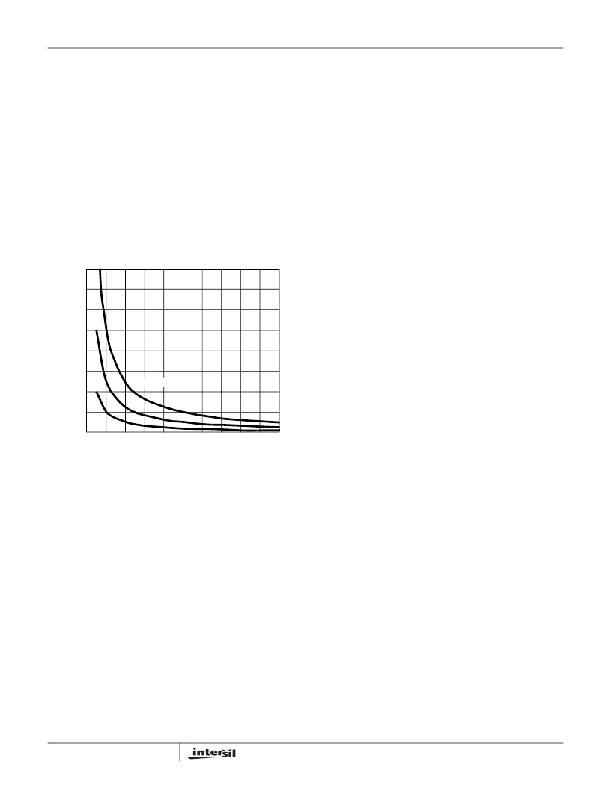
�FIGURE� 2.� BOOTSTRAP� CAPACITANCE� vs� BOOT� RIPPLE�
�VOLTAGE�
�The� bootstrap� capacitor� must� have� a� maximum� voltage�
�rating� well� above� the� maximum� voltage� intended� for� UVCC.�
�P� Qg_TOT� =� P� Qg_Q1� +� P� Qg_Q2� +� I� Q� ?� VCC�
�Q� G1� ?� UVCC� 2�
�V� GS1�
�(EQ.� 2)�
�C� BOOT_CAP� ≥� --------------------------------------�
�Q� GATE� =� ------------------------------------� ?� N� Q1�
�P� Qg_Q2� =� --------------------------------------� ?� F� SW� ?� N� Q2�
�I� DR� =� ?� ------------------------------------------------------� +� -----------------------------------------------------� ?� ?� F� SW� +� I� Q�
�Its� minimum� capacitance� value� can� be� chosen� from�
�Equation� 1.�
�Q� GATE�
�Δ� V� BOOT_CAP�
�Q� G1� ?� UVCC�
�V� GS1�
�(EQ.� 1)�
�Q� G2� ?� LVCC� 2�
�V� GS2�
�?� Q� G1� ?� UVCC� ?� N� Q1� Q� G2� ?� LVCC� ?� N� Q2� ?�
�?� V� GS1� V� GS2� ?�
�(EQ.� 3)�
�where� Q� G1� is� the� amount� of� gate� charge� per� upper� MOSFET�
�at� V� GS1� gate-source� voltage� and� N� Q1� is� the� number� of�
�control� MOSFETs.� The� Δ� V� BOOT_CAP� term� is� defined� as� the�
�allowable� droop� in� the� rail� of� the� upper� gate� drive.� Select�
�results� are� exemplified� in� Figure� 2.�
�Gate� Drive� Voltage� Versatility�
�The� ISL6622A� provides� the� user� flexibility� in� choosing� the�
�gate� drive� voltage� for� efficiency� optimization.� The� ISL6622A�
�7�
�where� the� gate� charge� (Q� G1� and� Q� G2� )� is� defined� at� a�
�particular� gate� to� source� voltage� (V� GS1� and� V� GS2� )� in� the�
�corresponding� MOSFET� data� sheet;� I� Q� is� the� driver� ’s� total�
�quiescent� current� with� no� load� at� both� drive� outputs;� N� Q1�
�and� N� Q2� are� number� of� upper� and� lower� MOSFETs,�
�respectively;� UVCC� and� LVCC� are� the� drive� voltages� for�
�both� upper� and� lower� FETs,� respectively.� The� I� Q*� VCC�
�product� is� the� quiescent� power� of� the� driver� without�
�capacitive� load.�
�FN6601.2�
�March� 19,� 2009�
�相关PDF资料 |
PDF描述 |
|---|---|
| ISL6622CBZ-T | IC MOSFET DVR SYNC BUCK 8-SOIC |
| ISL6801ABT | IC DRIVER HISIDE BOOTSTRAP 8SOIC |
| ISL78100ARZ | IC LED DRIVER AUTOMOTIVE 20-QFN |
| ISL8013AEVAL2Z | EVAL BOARD 2 FOR ISL8013A |
| ISL8014AEVAL2Z | EVAL BOARD 2 FOR ISL8014A |
相关代理商/技术参数 |
参数描述 |
|---|---|
| ISL6622AIBZ-T | 功能描述:IC MOSFET DRVR SYNC BUCK 8-SOIC RoHS:是 类别:集成电路 (IC) >> PMIC - MOSFET,电桥驱动器 - 外部开关 系列:- 标准包装:50 系列:- 配置:高端 输入类型:非反相 延迟时间:200ns 电流 - 峰:250mA 配置数:1 输出数:1 高端电压 - 最大(自引导启动):600V 电源电压:12 V ~ 20 V 工作温度:-40°C ~ 125°C 安装类型:通孔 封装/外壳:8-DIP(0.300",7.62mm) 供应商设备封装:8-DIP 包装:管件 其它名称:*IR2127 |
| ISL6622AIRZ | 功能描述:IC MOSFET DRVR SYNC BUCK 10-DFN RoHS:是 类别:集成电路 (IC) >> PMIC - MOSFET,电桥驱动器 - 外部开关 系列:- 标准包装:6,000 系列:* |
| ISL6622AIRZ-T | 功能描述:IC MOSFET DRVR SYNC BUCK 10-DFN RoHS:是 类别:集成电路 (IC) >> PMIC - MOSFET,电桥驱动器 - 外部开关 系列:- 标准包装:6,000 系列:* |
| ISL6622BCBZ | 制造商:Intersil Corporation 功能描述:PB-FREE SYNCH BUCK MOSFET HV DRIVER, NO LDO, VR11.1, 8LD SOI - Rail/Tube 制造商:Intersil Corporation 功能描述:Gate Drivers SYNCH BUCK MSFT HV DRVR NOLDO VR11 1 |
| ISL6622BCBZ-T | 制造商:Intersil Corporation 功能描述:PB-FREE SYNCH BUCK MOSFET HV DRIVER, NO LDO, VR11.1, 8LD SOI - Tape and Reel 制造商:Intersil Corporation 功能描述:Gate Drivers SYNCH BUCK MSFT HV DRVR NOLDO VR11 1 |
发布紧急采购,3分钟左右您将得到回复。