- 您现在的位置:买卖IC网 > Datasheet目录334 > ISL6622AIBZ (Intersil)IC MOSFET DRVR SYNC BUCK 8-SOIC Datasheet资料下载
参数资料
| 型号: | ISL6622AIBZ |
| 厂商: | Intersil |
| 文件页数: | 8/11页 |
| 文件大小: | 0K |
| 描述: | IC MOSFET DRVR SYNC BUCK 8-SOIC |
| 标准包装: | 980 |
| 配置: | 高端和低端,同步 |
| 输入类型: | PWM |
| 延迟时间: | 20ns |
| 电流 - 峰: | 1.25A |
| 配置数: | 1 |
| 输出数: | 2 |
| 高端电压 - 最大(自引导启动): | 36V |
| 电源电压: | 6.8 V ~ 13.2 V |
| 工作温度: | -40°C ~ 85°C |
| 安装类型: | 表面贴装 |
| 封装/外壳: | 8-SOIC(0.154",3.90mm 宽) |
| 供应商设备封装: | 8-SOIC |
| 包装: | 管件 |
�� �
�
�ISL6622A�
�P� DR� =� P� DR_UP� +� P� DR_LOW� +� I� Q� ?� VCC�
�P� DR_UP� =� ?� --------------------------------------� +� ----------------------------------------� ?� ?� ---------------------�
�?� R� HI1� +� R� EXT1� R� LO1� +� R� EXT1� ?�
�P� DR_LOW� =� ?� --------------------------------------� +� ----------------------------------------� ?� ?� ---------------------�
�?� R� HI2� +� R� EXT2� R� LO2� +� R� EXT2� ?�
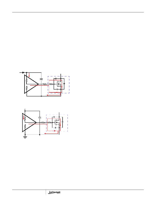
�The� total� gate� drive� power� losses� are� dissipated� among� the�
�resistive� components� along� the� transition� path,� as� outlined� in�
�Equation� 4.� The� drive� resistance� dissipates� a� portion� of� the�
�total� gate� drive� power� losses,� the� rest� will� be� dissipated� by� the�
�external� gate� resistors� (R� G1� and� R� G2� )� and� the� internal� gate�
�resistors� (R� GI1� and� R� GI2� )� of� MOSFETs.� Figures� 3� and� 4� show�
�the� typical� upper� and� lower� gate� drives� turn-on� current� path.�
�(EQ.� 4)�
�?� R� HI1� R� LO1� ?� P� Qg_Q1�
�2�
�?� R� HI2� R� LO2� ?� P� Qg_Q2�
�2�
�?� Minimize� trace� inductance,� especially� low-impedance�
�lines:� all� power� traces� (UGATE,� PHASE,� LGATE,� GND,�
�LVCC)� should� be� short� and� wide,� as� much� as� possible.�
�?� Minimize� the� inductance� of� the� PHASE� node:� ideally,� the�
�source� of� the� upper� and� the� drain� of� the� lower� MOSFET�
�should� be� as� close� as� thermally� allowable.�
�?� Minimize� the� input� current� loop:� connect� the� source� of� the�
�lower� MOSFET� to� ground� as� close� to� the� transistor� pin� as�
�feasible;� input� capacitors� (especially� ceramic� decoupling)�
�should� be� placed� as� close� to� the� drain� of� upper� and� source�
�of� lower� MOSFETs� as� possible.�
�In� addition,� for� improved� heat� dissipation,� place� copper�
�underneath� the� IC� whether� it� has� an� exposed� pad� or� not.� The�
�copper� area� can� be� extended� beyond� the� bottom� area� of� the�
�R� EXT1� =� R� G1� +� -------------�
�N�
�R� EXT2� =� R� G2� +� -------------�
�N�
�R� GI1�
�Q1�
�R� GI2�
�Q2�
�IC� and/or� connected� to� buried� power� ground� plane(s)� with�
�thermal� vias.� This� combination� of� vias� for� vertical� heat�
�escape,� extended� surface� copper� islands,� and� buried� planes�
�UVCC�
�BOOT�
�C� GD�
�D�
�combine� to� allow� the� IC� and� the� power� switches� to� achieve�
�their� full� thermal� potential.�
�Upper� MOSFET� Self� Turn-On� Effects� At� Startup�
�R� HI1�
�R� LO1�
�G�
�R� G1�
�R� GI1�
�C� GS�
�C� DS�
�Q1�
�Should� the� driver� have� insufficient� bias� voltage� applied,� its�
�outputs� are� floating.� If� the� input� bus� is� energized� at� a� high�
�dV/dt� rate� while� the� driver� outputs� are� floating,� due� to�
�self-coupling� via� the� internal� C� GD� of� the� MOSFET,� the� gate� of�
�S�
�PHASE�
�FIGURE� 3.� TYPICAL� UPPER-GATE� DRIVE� TURN-ON� PATH�
�LVCC�
�D�
�the� upper� MOSFET� could� momentarily� rise� up� to� a� level�
�greater� than� the� threshold� voltage� of� the� device,� potentially�
�turning� on� the� upper� switch.� Therefore,� if� such� a� situation�
�could� conceivably� be� encountered,� it� is� a� common� practice� to�
�place� a� resistor� (R� UGPH� )� across� the� gate� and� source� of� the�
�upper� MOSFET� to� suppress� the� Miller� coupling� effect.� The�
�value� of� the� resistor� depends� mainly� on� the� input� voltage’s�
�R� HI2�
�R� LO2�
�G�
�R� G2�
�C� GD�
�R� GI2�
�C� GS�
�C� DS�
�Q2�
�rate� of� rise,� the� C� GD� /C� GS� ratio,� as� well� as� the� gate-source�
�threshold� of� the� upper� MOSFET.� A� higher� dV/dt,� a� lower�
�C� DS� /C� GS� ratio,� and� a� lower� gate-source� threshold� upper� FET�
�will� require� a� smaller� resistor� to� diminish� the� effect� of� the�
�internal� capacitive� coupling.� For� most� applications,� the�
�integrated� 20k� Ω� resistor� is� sufficient,� not� affecting� normal�
�–� V�
�?�
�----------------------------------� ?�
�?� dV� ?�
�V� GS_MILLER� =� -------� ?� R� ?� C� rss� ?� 1� –� e� dt�
�iss� ?�
�-------� ?� R� ?� C�
�?� ?�
�?� ?�
�S�
�FIGURE� 4.� TYPICAL� LOWER-GATE� DRIVE� TURN-ON� PATH�
�Application� Information�
�Layout� Considerations�
�During� switching� of� the� devices,� the� parasitic� inductances� of�
�the� PCB� and� the� power� devices’� packaging� (both� upper� and�
�lower� MOSFETs)� leads� to� ringing,� possibly� in� excess� of� the�
�absolute� maximum� rating� of� the� devices.� Careful� layout� can�
�help� minimize� such� unwanted� stress.� The� following� advice� is�
�meant� to� lead� to� an� optimized� layout:�
�performance� and� efficiency.�
�The� coupling� effect� can� be� roughly� estimated� with�
�Equation� 5,� which� assumes� a� fixed� linear� input� ramp� and�
�neglects� the� clamping� effect� of� the� body� diode� of� the� upper�
�drive� and� the� bootstrap� capacitor.� Other� parasitic�
�components� such� as� lead� inductances� and� PCB�
�capacitances,� are� also� not� taken� into� account.� Figure� 5�
�provides� a� visual� reference� for� this� phenomenon� and� its�
�potential� solution.�
�DS�
�dV�
�(EQ.� 5)�
�dt�
�?� ?�
�?� Keep� decoupling� loops� (LVCC-GND� and� BOOT-PHASE)�
�as� short� as� possible.�
�8�
�R� =� R� UGPH� +� R� GI�
�C� rss� =� C� GD�
�C� iss� =� C� GD� +� C� GS�
�FN6601.2�
�March� 19,� 2009�
�相关PDF资料 |
PDF描述 |
|---|---|
| ISL6622CBZ-T | IC MOSFET DVR SYNC BUCK 8-SOIC |
| ISL6801ABT | IC DRIVER HISIDE BOOTSTRAP 8SOIC |
| ISL78100ARZ | IC LED DRIVER AUTOMOTIVE 20-QFN |
| ISL8013AEVAL2Z | EVAL BOARD 2 FOR ISL8013A |
| ISL8014AEVAL2Z | EVAL BOARD 2 FOR ISL8014A |
相关代理商/技术参数 |
参数描述 |
|---|---|
| ISL6622AIBZ-T | 功能描述:IC MOSFET DRVR SYNC BUCK 8-SOIC RoHS:是 类别:集成电路 (IC) >> PMIC - MOSFET,电桥驱动器 - 外部开关 系列:- 标准包装:50 系列:- 配置:高端 输入类型:非反相 延迟时间:200ns 电流 - 峰:250mA 配置数:1 输出数:1 高端电压 - 最大(自引导启动):600V 电源电压:12 V ~ 20 V 工作温度:-40°C ~ 125°C 安装类型:通孔 封装/外壳:8-DIP(0.300",7.62mm) 供应商设备封装:8-DIP 包装:管件 其它名称:*IR2127 |
| ISL6622AIRZ | 功能描述:IC MOSFET DRVR SYNC BUCK 10-DFN RoHS:是 类别:集成电路 (IC) >> PMIC - MOSFET,电桥驱动器 - 外部开关 系列:- 标准包装:6,000 系列:* |
| ISL6622AIRZ-T | 功能描述:IC MOSFET DRVR SYNC BUCK 10-DFN RoHS:是 类别:集成电路 (IC) >> PMIC - MOSFET,电桥驱动器 - 外部开关 系列:- 标准包装:6,000 系列:* |
| ISL6622BCBZ | 制造商:Intersil Corporation 功能描述:PB-FREE SYNCH BUCK MOSFET HV DRIVER, NO LDO, VR11.1, 8LD SOI - Rail/Tube 制造商:Intersil Corporation 功能描述:Gate Drivers SYNCH BUCK MSFT HV DRVR NOLDO VR11 1 |
| ISL6622BCBZ-T | 制造商:Intersil Corporation 功能描述:PB-FREE SYNCH BUCK MOSFET HV DRIVER, NO LDO, VR11.1, 8LD SOI - Tape and Reel 制造商:Intersil Corporation 功能描述:Gate Drivers SYNCH BUCK MSFT HV DRVR NOLDO VR11 1 |
发布紧急采购,3分钟左右您将得到回复。