- 您现在的位置:买卖IC网 > PDF目录15190 > ISL6741IBZ-T (Intersil)IC REG CTRLR PWM CM 16-SOIC PDF资料下载
参数资料
| 型号: | ISL6741IBZ-T |
| 厂商: | Intersil |
| 文件页数: | 22/28页 |
| 文件大小: | 0K |
| 描述: | IC REG CTRLR PWM CM 16-SOIC |
| 标准包装: | 2,500 |
| PWM 型: | 电流模式 |
| 输出数: | 2 |
| 频率 - 最大: | 2MHz |
| 占空比: | 100% |
| 电源电压: | 9 V ~ 16 V |
| 降压: | 无 |
| 升压: | 无 |
| 回扫: | 无 |
| 反相: | 无 |
| 倍增器: | 无 |
| 除法器: | 无 |
| Cuk: | 无 |
| 隔离: | 无 |
| 工作温度: | -40°C ~ 105°C |
| 封装/外壳: | 16-SOIC(0.154",3.90mm 宽) |
| 包装: | 带卷 (TR) |
第1页第2页第3页第4页第5页第6页第7页第8页第9页第10页第11页第12页第13页第14页第15页第16页第17页第18页第19页第20页第21页当前第22页第23页第24页第25页第26页第27页第28页
�� �
�
�ISL6740,� ISL6741�
�Other� duty� ranges� are� possible,� but� are� still� limited� to� a� 2:1� ratio.�
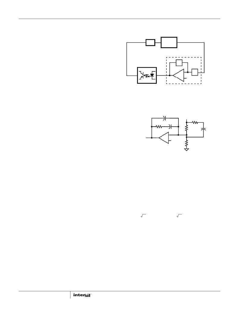
�A� block� diagram� of� the� feedback� control� loop� follows� in�
�The� voltage� applied� to� V� ERROR� must� be� scaled� to� the� peak-to-�
�peak� voltage� on� C� T� ,� and� offset� by� the� valley� voltage.� Since� the�
�peak-to-peak� C� T� voltage� is� 2.00V� nominal,� the� voltage� at� the�
�output� of� U100A� must� be� divided� by� 2.0V� to� obtain� the� desired�
�duty� cycle.� For� example,� if� an� 80%� duty� cycle� was� required� at� the�
�Figure� 19.�
�PWM�
�POWER�
�STAGE�
�V� OUT�
�minimum� operating� voltage,� the� output� of� U100A� must� be� 1.60V�
�(80%� of� 2.00V).� From� (Equation� 25),� the� divider� voltage� must� be�
�set� to� 1.4V� for� the� input� voltage� that� corresponds� to� the� 80%� duty�
�ERROR� AMPLIFIER�
�cycle.�
�ISOLATION�
�Z� 2�
�It� should� be� noted� that� the� synchronous� rectifiers� (SRs),� being�
�driven� from� the� transformer� secondary,� are� only� gated� on� during�
�the� ON� time� of� the� primary� FETs.� Conduction� continues� through�
�the� body� diodes� during� the� OFF� time� when� operating� in�
�-�
�+�
�REF�
�Z� 1�
�continuous� inductor� current� mode.� This� mode� of� operation�
�usually� results� in� significant� conduction� and� switching� losses� in�
�the� SR� FETs.� These� losses� may� be� reduced� considerably� by� either�
�adding� schottky� diodes� in� parallel� to� the� SR� FETs� or� by� driving� the�
�SR� FETs� directly� with� a� control� signal.�
�Adding� Regulation� -� Closed� Loop� Feedback�
�The� second� Typical� Application� schematic� adds� closed� loop�
�feedback� with� isolation.� The� ISL6740EVAL2Z� demonstration�
�platform� implements� this� design� and� is� available� for� evaluation.�
�The� input� voltage� range� was� increased� to� 36V� to� 75V,� which�
�FIGURE� 19.� CONTROL� LOOP� BLOCK� DIAGRAM�
�The� loop� compensation� is� placed� around� the� Error� Amplifier� (EA)�
�on� the� secondary� side� of� the� converter.� A� Type� 3� error� amplifier�
�configuration� was� selected.�
�V� OUT�
�necessitates� a� few� modifications� to� the� open� loop� design.� The�
�output� inductor� value� was� increased� to� 4.0� μ� H,� schottky� rectifier�
�V� ERR�
�-�
�+�
�REF�
�CR4� was� added� to� minimize� SR� FET� body� diode� conduction,� the�
�turns� ratio� of� the� main� transformer� was� changed� to� 4:3,� and� the�
�synchronous� rectifier� gate� drives� were� modified.� The� design�
�process� is� essentially� the� same� as� it� was� for� the� unregulated�
�version,� so� only� the� feedback� control� loop� design� will� be�
�discussed.�
�FIGURE� 20.� TYPE� 3� ERROR� AMPLIFIER�
�The� control� to� output� transfer� function� may� be� represented� as� [1]�
�1� +� ------�
�v� o� V� IN� N� S� ω� z�
�V� S� ?� 2�
�1� +� ----------------� +� ?� -------� ?�
�(� Q� )ω� ?� ω� ?�
�R� o�
�ω� o� ?� L�
�The� major� components� of� the� feedback� control� loop� are� a�
�programmable� shunt� regulator� and� an� opto-coupler.� The� opto-�
�coupler� is� used� to� transfer� the� error� signal� across� the� isolation�
�barrier.� The� opto-coupler� offers� a� convenient� means� to� cross� the�
�isolation� barrier,� but� it� adds� complexity� to� the� feedback� control�
�loop.� It� adds� a� pole� at� about� 10kHz� and� a� significant� amount� of�
�gain� variation� due� the� current� transfer� ratio� (CTR).� The� CTR� of� the�
�opto-coupler� varies� with� initial� tolerance,� temperature,� forward�
�current,� and� age.�
�s�
�-----� =� ---------------� ?� -------� ?� ------------------------------------------------�
�v� c� N� P� s� s� 2�
�o� o�
�where:�
�Q� =� ---------------�
�(EQ.� 26)�
�ω� o� =� -----------�
�f� o� =� ------------------�
�ω� z� =� ----------�
�f� z� =� ------------------�
�1�
�LC�
�1�
�R� c� C�
�or�
�or�
�1�
�2� π� LC�
�1�
�2� π� R� c� C�
�R� o� =� Output� Load� Resistance�
�L� =� Output� Inductance�
�C� =� Output� Capacitance�
�R� c� =� Output� Capacitance� ESR�
�V� S� =� Sawtooth� Ramp� Amplitude�
�Gain� and� phase� plots� of� (Equation� 26)� appear� below� using�
�L� =� 4.0� μ� H,� C� =� 150� μ� F,� Rc� =� 28m� Ω� ,� Ro� =� 1.2� Ω� ,� and� VIN� =� 75V.�
�22�
�FN9111.6�
�December� 2,� 2011�
�相关PDF资料 |
PDF描述 |
|---|---|
| ISL6745AUZ-T | IC REG CTRLR PWM VM 10-MSOP |
| ISL6269AIRZ-T | IC REG CTRLR BUCK PWM 16-QFN |
| H2BXG-10112-Y8-ND | JUMPER-H1501TR/A3048Y/X 12" |
| ISL6445IAZ-TK | IC REG CTRLR BUCK PWM CM 24-QSOP |
| H2BXG-10112-W8-ND | JUMPER-H1501TR/A3048W/X 12" |
相关代理商/技术参数 |
参数描述 |
|---|---|
| ISL6741IV | 功能描述:IC REG CTRLR PWM CM 16-TSSOP RoHS:否 类别:集成电路 (IC) >> PMIC - 稳压器 - DC DC 切换控制器 系列:- 标准包装:2,500 系列:- PWM 型:电流模式 输出数:1 频率 - 最大:500kHz 占空比:100% 电源电压:8.2 V ~ 30 V 降压:无 升压:无 回扫:是 反相:无 倍增器:无 除法器:无 Cuk:无 隔离:是 工作温度:0°C ~ 70°C 封装/外壳:8-DIP(0.300",7.62mm) 包装:管件 产品目录页面:1316 (CN2011-ZH PDF) |
| ISL6741IV-T | 功能描述:IC REG CTRLR PWM CM 16-TSSOP RoHS:否 类别:集成电路 (IC) >> PMIC - 稳压器 - DC DC 切换控制器 系列:- 标准包装:2,500 系列:- PWM 型:电流模式 输出数:1 频率 - 最大:500kHz 占空比:100% 电源电压:8.2 V ~ 30 V 降压:无 升压:无 回扫:是 反相:无 倍增器:无 除法器:无 Cuk:无 隔离:是 工作温度:0°C ~ 70°C 封装/外壳:8-DIP(0.300",7.62mm) 包装:管件 产品目录页面:1316 (CN2011-ZH PDF) |
| ISL6741IVZ | 功能描述:IC REG CTRLR PWM CM 16-TSSOP RoHS:是 类别:集成电路 (IC) >> PMIC - 稳压器 - DC DC 切换控制器 系列:- 产品培训模块:Lead (SnPb) Finish for COTS Obsolescence Mitigation Program 标准包装:2,500 系列:- PWM 型:电流模式 输出数:1 频率 - 最大:275kHz 占空比:50% 电源电压:18 V ~ 110 V 降压:无 升压:无 回扫:无 反相:无 倍增器:无 除法器:无 Cuk:无 隔离:是 工作温度:-40°C ~ 85°C 封装/外壳:8-SOIC(0.154",3.90mm 宽) 包装:带卷 (TR) |
| ISL6741IVZ-T | 功能描述:IC REG CTRLR PWM CM 16-TSSOP RoHS:是 类别:集成电路 (IC) >> PMIC - 稳压器 - DC DC 切换控制器 系列:- 产品培训模块:Lead (SnPb) Finish for COTS Obsolescence Mitigation Program 标准包装:2,500 系列:- PWM 型:电流模式 输出数:1 频率 - 最大:275kHz 占空比:50% 电源电压:18 V ~ 110 V 降压:无 升压:无 回扫:无 反相:无 倍增器:无 除法器:无 Cuk:无 隔离:是 工作温度:-40°C ~ 85°C 封装/外壳:8-SOIC(0.154",3.90mm 宽) 包装:带卷 (TR) |
| ISL6742AAZA | 功能描述:IC REG CTRLR PWM CM/VM 16-QSOP RoHS:是 类别:集成电路 (IC) >> PMIC - 稳压器 - DC DC 切换控制器 系列:- 标准包装:75 系列:- PWM 型:电流模式 输出数:1 频率 - 最大:1MHz 占空比:81% 电源电压:4.3 V ~ 13.5 V 降压:是 升压:是 回扫:是 反相:无 倍增器:无 除法器:无 Cuk:无 隔离:无 工作温度:0°C ~ 70°C 封装/外壳:8-SOIC(0.154",3.90mm 宽) 包装:管件 产品目录页面:1051 (CN2011-ZH PDF) 其它名称:296-2543-5 |
发布紧急采购,3分钟左右您将得到回复。