- 您现在的位置:买卖IC网 > PDF目录15524 > ISL6752AAZA (Intersil)IC REG CTRLR PWM CM 16-QSOP PDF资料下载
参数资料
| 型号: | ISL6752AAZA |
| 厂商: | Intersil |
| 文件页数: | 8/16页 |
| 文件大小: | 0K |
| 描述: | IC REG CTRLR PWM CM 16-QSOP |
| 标准包装: | 98 |
| PWM 型: | 电流模式 |
| 输出数: | 6 |
| 频率 - 最大: | 2MHz |
| 占空比: | 100% |
| 电源电压: | 9 V ~ 16 V |
| 降压: | 无 |
| 升压: | 无 |
| 回扫: | 无 |
| 反相: | 无 |
| 倍增器: | 无 |
| 除法器: | 无 |
| Cuk: | 无 |
| 隔离: | 无 |
| 工作温度: | -40°C ~ 105°C |
| 封装/外壳: | 16-SSOP(0.154",3.90mm 宽) |
| 包装: | 管件 |
| 产品目录页面: | 1243 (CN2011-ZH PDF) |
�� �
�
�ISL6752�
�Typical� Performance� Curves�
�(Continued)�
�1-10� 4�
�1-10� 3�
�CT = 680pF�
�CT = 1000pF�
�1-10� 3�
�RTD = 10k� Ω�
�100�
�CT = 470pF�
�CT = 330pF�
�CT = 220pF�
�CT = 100pF�
�100�
�RTD = 100k� Ω�
�RTD = 50k� Ω�
�10�
�0�
�10�
�20�
�30�
�40� 50� 60�
�RTD� (k� Ω� )�
�70�
�80�
�90�
�100�
�10�
�0.1�
�1�
�CT� (nF)�
�10�
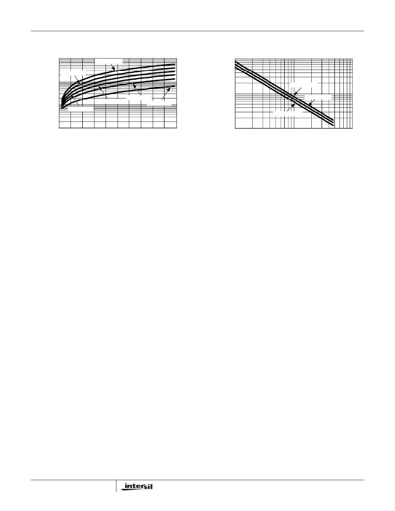
�FIGURE� 3.� DEADTIME� (DT)� vs� CAPACITANCE�
�Pin� Descriptions�
�VDD� -� VDD� is� the� power� connection� for� the� IC.� To� optimize�
�noise� immunity,� bypass� VDD� to� GND� with� a� ceramic�
�capacitor� as� close� to� the� VDD� and� GND� pins� as� possible.�
�VDD� is� monitored� for� supply� voltage� undervoltage� lock-out�
�(UVLO).� The� start� and� stop� thresholds� track� each� other�
�resulting� in� relatively� constant� hysteresis.�
�GND� -� Signal� and� power� ground� connections� for� this� device.�
�Due� to� high� peak� currents� and� high� frequency� operation,� a�
�low� impedance� layout� is� necessary.� Ground� planes� and�
�short� traces� are� highly� recommended.�
�VREF� -� The� 5.00V� reference� voltage� output� having� 3%�
�tolerance� over� line,� load� and� operating� temperature.� Bypass�
�to� GND� with� a� 0.1μF� to� 2.2μF� low� ESR� capacitor.�
�CT� -� The� oscillator� timing� capacitor� is� connected� between�
�this� pin� and� GND.� It� is� charged� through� an� internal� 200μA�
�current� source� and� discharged� with� a� user� adjustable� current�
�source� controlled� by� RTD.�
�RTD� -� This� is� the� oscillator� timing� capacitor� discharge�
�current� control� pin.� The� current� flowing� in� a� resistor�
�connected� between� this� pin� and� GND� determines� the�
�magnitude� of� the� current� that� discharges� CT.� The� CT�
�discharge� current� is� nominally� 20x� the� resistor� current.� The�
�PWM� deadtime� is� determined� by� the� timing� capacitor�
�discharge� duration.� The� voltage� at� RTD� is� nominally� 2V.�
�CS� -� This� is� the� input� to� the� overcurrent� comparator.� The�
�overcurrent� comparator� threshold� is� set� at� 1V� nominal.� The�
�CS� pin� is� shorted� to� GND� at� the� termination� of� either� PWM�
�output.�
�Depending� on� the� current� sensing� source� impedance,� a�
�series� input� resistor� may� be� required� due� to� the� delay�
�between� the� internal� clock� and� the� external� power� switch.�
�This� delay� may� result� in� CS� being� discharged� prior� to� the�
�power� switching� device� being� turned� off.�
�8�
�FIGURE� 4.� CAPACITANCE� vs� FREQUENCY�
�OUTUL� and� OUTUR� -� These� outputs� control� the� upper�
�bridge� FETs� and� operate� at� a� fixed� 50%� duty� cycle� in�
�alternate� sequence.� OUTUL� controls� the� upper� left� FET� and�
�OUTUR� controls� the� upper� right� FET.� The� left� and� right�
�designation� may� be� switched� as� long� as� they� are� switched� in�
�conjunction� with� the� lower� FET� outputs,� OUTLL� and� OUTLR.�
�RESDEL� -� Sets� the� resonant� delay� period� between� the�
�toggle� of� the� upper� FETs� and� the� turn� on� of� either� of� the�
�lower� FETs.� The� voltage� applied� to� RESDEL� determines�
�when� the� upper� FETs� switch� relative� to� a� lower� FET� turning�
�on.� Varying� the� control� voltage� from� 0V� to� 2V� increases� the�
�resonant� delay� duration� from� 0� to� 100%� of� the� deadtime.� The�
�control� voltage� divided� by� 2� represents� the� percent� of� the�
�deadtime� equal� to� the� resonant� delay.� In� practice� the�
�maximum� resonant� delay� must� be� set� lower� than� 2V� to�
�ensure� that� the� lower� FETs,� at� maximum� duty� cycle,� are� OFF�
�prior� to� the� switching� of� the� upper� FETs.�
�OUTLL� and� OUTLR� -� These� outputs� control� the� lower� bridge�
�FETs,� are� pulse� width� modulated,� and� operate� in� alternate�
�sequence.� OUTLL� controls� the� lower� left� FET� and� OUTLR�
�controls� the� lower� right� FET.� The� left� and� right� designation�
�may� be� switched� as� long� as� they� are� switched� in� conjunction�
�with� the� upper� FET� outputs,� OUTUL� and� OUTUR.�
�OUTLLN� and� OUTLRN� -� These� outputs� are� the�
�complements� of� the� PWM� (lower)� bridge� FETs.� OUTLLN� is�
�the� complement� of� OUTLL� and� OUTLRN� is� the� complement�
�of� OUTLR.� These� outputs� are� suitable� for� control� of�
�synchronous� rectifiers.� The� phase� relationship� between�
�each� output� and� its� complement� is� controlled� by� the� voltage�
�applied� to� VADJ.�
�VADJ� -� A� 0V� to� 5V� control� voltage� applied� to� this� input� sets�
�the� relative� delay� or� advance� between� OUTLL/OUTLR� and�
�OUTLLN/OUTLRN.� The� phase� relationship� between�
�OUTUL/OUTUR� and� OUTLL/OUTLR� is� maintained�
�regardless� of� the� phase� adjustment� between� OUTLL/OUTLR�
�and� OUTLLN/OUTLRN.�
�FN9181.3�
�October� 31,� 2008�
�相关PDF资料 |
PDF描述 |
|---|---|
| 0925-273K | COIL RF 27UH MOLDED SHIELDED |
| VI-J60-EY | CONVERTER MOD DC/DC 5V 50W |
| RMM08DTAT | CONN EDGECARD 16POS R/A .156 SLD |
| 0819-96K | COIL RF 1000UH MOLDED UNSHIELDED |
| VI-J5F-EY | CONVERTER MOD DC/DC 72V 50W |
相关代理商/技术参数 |
参数描述 |
|---|---|
| ISL6752AAZAR5325 | 制造商:Intersil Corporation 功能描述:- Rail/Tube |
| ISL6752AAZA-T | 功能描述:IC REG CTRLR PWM CM 16-QSOP RoHS:是 类别:集成电路 (IC) >> PMIC - 稳压器 - DC DC 切换控制器 系列:- 产品培训模块:Lead (SnPb) Finish for COTS Obsolescence Mitigation Program 标准包装:2,500 系列:- PWM 型:电流模式 输出数:1 频率 - 最大:275kHz 占空比:50% 电源电压:18 V ~ 110 V 降压:无 升压:无 回扫:无 反相:无 倍增器:无 除法器:无 Cuk:无 隔离:是 工作温度:-40°C ~ 85°C 封装/外壳:8-SOIC(0.154",3.90mm 宽) 包装:带卷 (TR) |
| ISL6752AAZA-TR5325 | 制造商:Intersil Corporation 功能描述:ZVS Full-Bridge Current-Mode PWM with Adjustable Synchronous Rectifier Control |
| ISL6752DBEVAL1Z | 功能描述:BOARD DEMO FOR ISL6752 RoHS:是 类别:编程器,开发系统 >> 评估板 - DC/DC 与 AC/DC(离线)SMPS 系列:* 标准包装:1 系列:- 主要目的:DC/DC,步降 输出及类型:1,非隔离 功率 - 输出:- 输出电压:3.3V 电流 - 输出:3A 输入电压:4.5 V ~ 28 V 稳压器拓扑结构:降压 频率 - 开关:250kHz 板类型:完全填充 已供物品:板 已用 IC / 零件:L7981 其它名称:497-12113STEVAL-ISA094V1-ND |
| ISL6752EVAL1Z | 功能描述:EVALUATION BOARD FOR ISL6752 RoHS:是 类别:编程器,开发系统 >> 过时/停产零件编号 系列:- 标准包装:1 系列:- 传感器类型:CMOS 成像,彩色(RGB) 传感范围:WVGA 接口:I²C 灵敏度:60 fps 电源电压:5.7 V ~ 6.3 V 嵌入式:否 已供物品:成像器板 已用 IC / 零件:KAC-00401 相关产品:4H2099-ND - SENSOR IMAGE WVGA COLOR 48-PQFP4H2094-ND - SENSOR IMAGE WVGA MONO 48-PQFP |
发布紧急采购,3分钟左右您将得到回复。