- 您现在的位置:买卖IC网 > PDF目录15524 > ISL6752AAZA (Intersil)IC REG CTRLR PWM CM 16-QSOP PDF资料下载
参数资料
| 型号: | ISL6752AAZA |
| 厂商: | Intersil |
| 文件页数: | 9/16页 |
| 文件大小: | 0K |
| 描述: | IC REG CTRLR PWM CM 16-QSOP |
| 标准包装: | 98 |
| PWM 型: | 电流模式 |
| 输出数: | 6 |
| 频率 - 最大: | 2MHz |
| 占空比: | 100% |
| 电源电压: | 9 V ~ 16 V |
| 降压: | 无 |
| 升压: | 无 |
| 回扫: | 无 |
| 反相: | 无 |
| 倍增器: | 无 |
| 除法器: | 无 |
| Cuk: | 无 |
| 隔离: | 无 |
| 工作温度: | -40°C ~ 105°C |
| 封装/外壳: | 16-SSOP(0.154",3.90mm 宽) |
| 包装: | 管件 |
| 产品目录页面: | 1243 (CN2011-ZH PDF) |
�� �
�
�ISL6752�
�Voltages� below� 2.425V� result� in� OUTLLN/OUTLRN� being�
�advanced� relative� to� OUTLL/OUTLR.� Voltages� above�
�2.575V� result� in� OUTLLN/OUTLRN� being� delayed� relative� to�
�OUTLL/OUTLR.� A� voltage� of� 2.50V� ±75mV� results� in� zero�
�The� switching� period� is� the� sum� of� the� timing� capacitor�
�charge� and� discharge� durations.� The� charge� duration� is�
�determined� by� CT� and� a� fixed� 200μA� internal� current� source.�
�The� discharge� duration� is� determined� by� RTD� and� CT.�
�t� C� ≈� 11.5� ?� 10� ?� CT�
�phase� difference.� A� weak� internal� 50%� divider� from� VREF�
�results� in� no� phase� delay� if� this� input� is� left� floating.�
�3�
�S�
�(EQ.� 1)�
�The� range� of� phase� delay/advance� is� either� zero� or� 40ns� to�
�t� D� ≈� (� 0.06� ?� RTD� ?� CT� )� +� 50� ?� 10�
�–� 9�
�S�
�(EQ.� 2)�
�300ns� with� the� phase� differential� increasing� as� the� voltage�
�t� SW� =� t� C� +� t� D� =� ------------�
�deviation� from� 2.5V� increases.� The� relationship� between� the�
�control� voltage� and� phase� differential� is� non-linear.� The� gain�
�1�
�F� SW�
�S�
�(EQ.� 3)�
�(� Δ� t/� Δ� V)� is� low� for� control� voltages� near� 2.5V� and� rapidly�
�increases� as� the� voltage� approaches� the� extremes� of� the�
�control� range.� This� behavior� provides� the� user� increased�
�accuracy� when� selecting� a� shorter� delay/advance� duration.�
�When� the� PWM� outputs� are� delayed� relative� to� the� SR�
�outputs� (VADJ� <� 2.425V),� the� delay� time� should� not� exceed�
�90%� of� the� deadtime� as� determined� by� RTD� and� CT.�
�VERR� -� The� control� voltage� input� to� the� inverting� input� of� the�
�PWM� comparator.� The� output� of� an� external� error� amplifier�
�(EA)� is� applied� to� this� input,� either� directly� or� through� an�
�opto-coupler,� for� closed� loop� regulation.� VERR� has� a�
�nominal� 1mA� pull-up� current� source.�
�CTBUF� -� CTBUF� is� the� buffered� output� of� the� sawtooth�
�oscillator� waveform� present� on� CT� and� is� capable� of�
�sourcing� 2mA.� It� is� offset� from� ground� by� 0.40V� and� has� a�
�nominal� valley-to-peak� gain� of� 2.� It� may� be� used� for� slope�
�where� t� C� and� t� D� are� the� charge� and� discharge� times,�
�respectively,� CT� is� the� timing� capacitor� in� Farads,� RTD� is� the�
�discharge� programming� resistance� in� ohms,� t� SW� is� the�
�oscillator� period,� and� F� SW� is� the� oscillator� frequency.� One�
�output� switching� cycle� requires� two� oscillator� cycles.� The�
�actual� times� will� be� slightly� longer� than� calculated� due� to�
�internal� propagation� delays� of� approximately� 10ns/transition.�
�This� delay� adds� directly� to� the� switching� duration,� but� also�
�causes� overshoot� of� the� timing� capacitor� peak� and� valley�
�voltage� thresholds,� effectively� increasing� the� peak-to-peak�
�voltage� on� the� timing� capacitor.� Additionally,� if� very� small�
�discharge� currents� are� used,� there� will� be� increased� error�
�due� to� the� input� impedance� at� the� CT� pin.� The� maximum�
�recommended� current� through� RTD� is� 1mA,� which� produces�
�a� CT� discharge� current� of� 20mA.�
�The� maximum� duty� cycle,� D,� and� percent� deadtime,� DT,� can�
�be� calculated� from� Equations� 4� and� 5:�
�t� C�
�compensation.�
�Functional� Description�
�Features�
�The� ISL6752� PWM� is� an� excellent� choice� for� low� cost� ZVS�
�D� =� ----------�
�t� SW�
�DT� =� 1� –� D�
�(EQ.� 4)�
�(EQ.� 5)�
�full-bridge� applications� requiring� adjustable� synchronous�
�rectifier� drive.� With� its� many� protection� and� control� features,�
�a� highly� flexible� design� with� minimal� external� components� is�
�possible.� Among� its� many� features� are� a� very� accurate�
�overcurrent� limit� threshold,� thermal� protection,� a� buffered�
�sawtooth� oscillator� output� suitable� for� slope� compensation,�
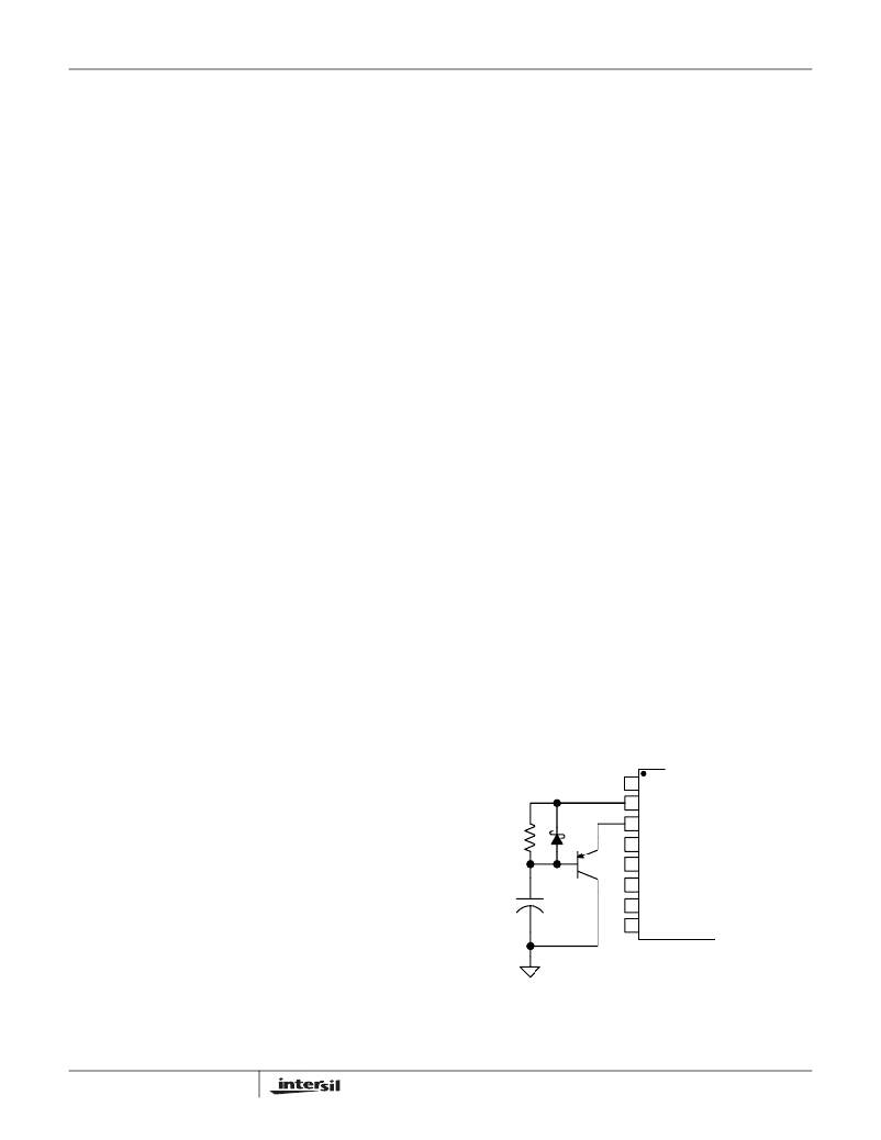
�Implementing� Soft-Start�
�The� ISL6752� does� not� have� a� soft-start� feature.� Soft-start�
�can� be� implemented� externally� using� the� components� shown�
�in� the� following.� The� RC� network� governs� the� rate� of� rise� of�
�the� transistor� ’s� base,� which� clamps� the� voltage� at� VERR.�
�synchronous� rectifier� outputs� with� variable� delay/advance�
�timing,� and� adjustable� frequency.�
�If� synchronous� rectification� is� not� required,� please� consider�
�1�
�2� VREF�
�3� VERR�
�1�
�5�
�1�
�1�
�6�
�the� ISL6753� controller.�
�R�
�4�
�4�
�1�
�Oscillator�
�The� ISL6752� has� an� oscillator� with� a� programmable�
�5�
�6�
�ISL6752�
�3�
�1�
�2�
�1�
�frequency� range� to� 2MHz,� which� can� be� programmed� with� a�
�resistor� and� capacitor.�
�C�
�7�
�8�
�1�
�1�
�0�
�9�
�FIGURE� 5.� IMPLEMENTING� SOFT-START�
�9�
�FN9181.3�
�October� 31,� 2008�
�相关PDF资料 |
PDF描述 |
|---|---|
| 0925-273K | COIL RF 27UH MOLDED SHIELDED |
| VI-J60-EY | CONVERTER MOD DC/DC 5V 50W |
| RMM08DTAT | CONN EDGECARD 16POS R/A .156 SLD |
| 0819-96K | COIL RF 1000UH MOLDED UNSHIELDED |
| VI-J5F-EY | CONVERTER MOD DC/DC 72V 50W |
相关代理商/技术参数 |
参数描述 |
|---|---|
| ISL6752AAZAR5325 | 制造商:Intersil Corporation 功能描述:- Rail/Tube |
| ISL6752AAZA-T | 功能描述:IC REG CTRLR PWM CM 16-QSOP RoHS:是 类别:集成电路 (IC) >> PMIC - 稳压器 - DC DC 切换控制器 系列:- 产品培训模块:Lead (SnPb) Finish for COTS Obsolescence Mitigation Program 标准包装:2,500 系列:- PWM 型:电流模式 输出数:1 频率 - 最大:275kHz 占空比:50% 电源电压:18 V ~ 110 V 降压:无 升压:无 回扫:无 反相:无 倍增器:无 除法器:无 Cuk:无 隔离:是 工作温度:-40°C ~ 85°C 封装/外壳:8-SOIC(0.154",3.90mm 宽) 包装:带卷 (TR) |
| ISL6752AAZA-TR5325 | 制造商:Intersil Corporation 功能描述:ZVS Full-Bridge Current-Mode PWM with Adjustable Synchronous Rectifier Control |
| ISL6752DBEVAL1Z | 功能描述:BOARD DEMO FOR ISL6752 RoHS:是 类别:编程器,开发系统 >> 评估板 - DC/DC 与 AC/DC(离线)SMPS 系列:* 标准包装:1 系列:- 主要目的:DC/DC,步降 输出及类型:1,非隔离 功率 - 输出:- 输出电压:3.3V 电流 - 输出:3A 输入电压:4.5 V ~ 28 V 稳压器拓扑结构:降压 频率 - 开关:250kHz 板类型:完全填充 已供物品:板 已用 IC / 零件:L7981 其它名称:497-12113STEVAL-ISA094V1-ND |
| ISL6752EVAL1Z | 功能描述:EVALUATION BOARD FOR ISL6752 RoHS:是 类别:编程器,开发系统 >> 过时/停产零件编号 系列:- 标准包装:1 系列:- 传感器类型:CMOS 成像,彩色(RGB) 传感范围:WVGA 接口:I²C 灵敏度:60 fps 电源电压:5.7 V ~ 6.3 V 嵌入式:否 已供物品:成像器板 已用 IC / 零件:KAC-00401 相关产品:4H2099-ND - SENSOR IMAGE WVGA COLOR 48-PQFP4H2094-ND - SENSOR IMAGE WVGA MONO 48-PQFP |
发布紧急采购,3分钟左右您将得到回复。