- 您现在的位置:买卖IC网 > PDF目录15495 > ISL8118CRZ (Intersil)IC REG CTRLR BUCK PWM VM 28-QFN PDF资料下载
参数资料
| 型号: | ISL8118CRZ |
| 厂商: | Intersil |
| 文件页数: | 13/20页 |
| 文件大小: | 0K |
| 描述: | IC REG CTRLR BUCK PWM VM 28-QFN |
| 标准包装: | 60 |
| PWM 型: | 电压模式 |
| 输出数: | 1 |
| 频率 - 最大: | 2MHz |
| 占空比: | 100% |
| 电源电压: | 2.97 V ~ 22 V |
| 降压: | 是 |
| 升压: | 无 |
| 回扫: | 无 |
| 反相: | 无 |
| 倍增器: | 无 |
| 除法器: | 无 |
| Cuk: | 无 |
| 隔离: | 无 |
| 工作温度: | 0°C ~ 70°C |
| 封装/外壳: | 28-VFQFN 裸露焊盘 |
| 包装: | 管件 |
| 产品目录页面: | 1244 (CN2011-ZH PDF) |
�� �
�
�ISL8118�
�Sinking� OCP� faults� cause� the� bottom� side� MOSFET� drive� to�
�Fs� [� Hz� ]� ≈� 1.178� ×� 10�
�be� disabled,� effectively� operating� the� ISL8118� in� a�
�10�
�?� R� T� [� Ω� ]�
�–� 0.973�
�(R� T� TO� GND)�
�(EQ.� 2)�
�non-synchronous� manner.� The� fault� is� maintained� for� three�
�clock� cycles� at� which� point� it� is� cleared� and� normal� operation�
�is� restored.� OVP� fault� implementation� overrides� sourcing�
�and� sinking� OCP� events,� immediately� turning� on� the� bottom�
�side� MOSFET� and� turning� off� the� top� side� MOSFET.� The� OC�
�trip� point� varies� mainly� due� to� the� MOSFETs� rDS(ON)�
�variations� and� system� noise.� To� avoid� overcurrent� tripping� in�
�the� normal� operating� load� range,� find� the� RTSOC� and/or�
�RBSOC� resistor� from� the� previous� detailed� equations� with:�
�1.� Maximum� rDS(ON)� at� the� highest� junction� temperature;�
�2.� Minimum� IBSOC� and/or� ITSOC� from� specification� table;�
�3.� Determine� the� overcurrent� trip� point� greater� than� the�
�maximum� output� continuous� current� at� maximum�
�inductor� ripple� current.�
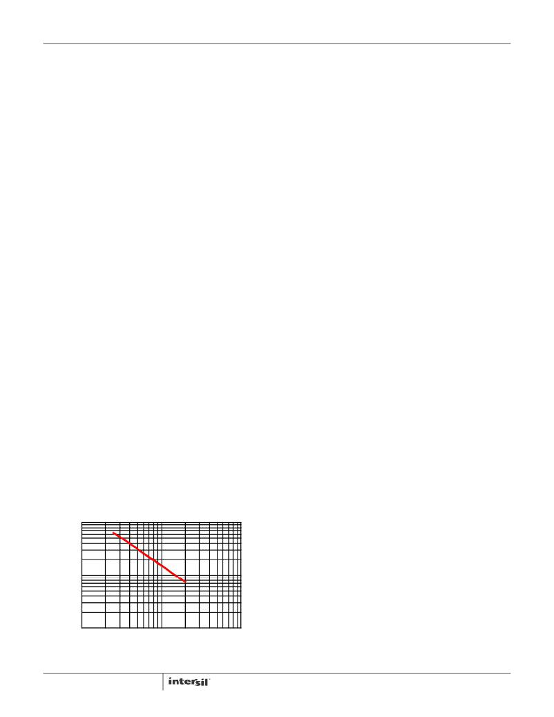
�Frequency� Programming�
�By� tying� a� resistor� to� GND� from� FSET� pin,� the� switching�
�frequency� can� be� set� between� 250kHz� and� 2MHz.�
�Oscillator/VFF�
�The� Oscillator� is� a� triangle� waveform,� providing� for� leading�
�and� falling� edge� modulation.� The� bottom� of� the� oscillator�
�waveform� is� set� at� 1.0V.� The� ramp's� peak-to-peak� amplitude�
�is� determined� from� the� voltage� on� the� VFF� (Voltage� Feed�
�Forward)� pin� by� Equation� 1:�
�Internal� Series� Linear� Regulator�
�The� VIN� pin� is� connected� to� PVCC� with� a� 2� Ω� internal� series�
�linear� regulator,� which� is� internally� compensated.� The� external�
�Series� Linear� regulator� option� should� be� used� for� applications�
�requiring� pass� elements� of� less� than� 2� Ω� .� When� using� the�
�internal� regulator,� the� EXDRV� pin� should� be� connected� directly�
�to� GND.� The� PVCC� and� VIN� pins� should� have� a� bypass�
�capacitor� (at� least� 10μF� on� PVCC� is� required)� connected� to�
�PGND.� For� proper� operation,� the� PVCC� capacitor� must� be�
�within� 150� mils� of� the� PVCC� and� the� PGND� pins,� and� be�
�connected� to� these� pins� with� dedicated� traces.� The� internal�
�series� linear� regulator’s� input� (VIN)� can� range� between� 3.3V� to�
�20V� ±10%.� The� internal� linear� regulator� is� to� provide� power� for�
�both� the� internal� MOSFET� drivers� through� the� PVCC� pin� and�
�the� analog� circuitry� through� the� VCC� pin.� The� VCC� pin� should�
�be� connected� to� the� PVCC� pin� with� an� RC� filter� to� prevent� high�
�frequency� driver� switching� noise� from� entering� the� analog�
�circuitry.� When� VIN� drops� below� 5.6V,� the� pass� element� will�
�saturate;� PVCC� will� track� VIN,� minus� the� dropout� of� the� linear�
�regulator:� PVCC� =� VIN-2xIVIN.� When� used� with� an� external� 5V�
�supply,� the� VIN� pin� should� be� tied� directly� to� PVCC.�
�External� Series� Linear� Regulator�
�The� EXDRV� pin� provides� sinking� drive� capability� for� an�
�external� pass� element� linear� regulator� controller.� The�
�D� VOSC� =� 0.16� ?� VFF�
�(EQ.� 1)�
�external� linear� options� are� especially� useful� when� the�
�An� internal� RC� filter� of� 233k� Ω� and� 2pF� (341kHz)� provides�
�filtering� of� the� VFF� voltage.� An� external� RC� filter� may� be�
�required� to� augment� this� filter� in� the� event� that� it� is� insufficient� to�
�prevent� noise� injection� or� control� loop� interactions.� Voltages�
�below� 2.9V� on� the� VFF� pin� may� result� in� undesirable� operation�
�due� to� extremely� small� peak-to-peak� oscillator� waveforms.� The�
�oscillator� waveform� should� not� exceed� VCC� -1.0V.� For� high�
�VFF� voltages� the� internal/external� 5.6V� linear� regulator� should�
�be� used.� 5.6V� on� VCC� provides� sufficient� headroom� for� 100%�
�duty� cycle� operation� when� using� the� maximum� VFF� voltage� of�
�22V.� In� the� event� of� sustained� 100%� duty� cycle� operation,�
�defined� as� 32� clock� cycles� where� no� BG� pulse� is� detected,� BG�
�will� be� pulsed� on� to� refresh� the� design’s� Bootstrap� capacitor.�
�100�
�10�
�internal� linear� dropout� is� too� large� for� a� given� application.�
�When� using� the� external� linear� regulator� option,� the� EXDRV�
�pin� should� be� connected� to� the� gate� of� a� PMOS� device,� and�
�a� resistor� should� be� connected� between� its� gate� and� source.�
�A� resistor� and� a� capacitor� should� be� connected� from� gate� to�
�source� to� compensate� the� control� loop.� A� PNP� device� can� be�
�used� instead� of� a� PMOS� device,� in� which� case� the� EXDRV�
�pin� should� be� connected� to� the� base� of� the� PNP� pass�
�element.� The� maximum� sinking� capability� of� the� EXDRV� pin�
�is� 0.5mA,� and� should� not� be� exceeded� if� using� an� external�
�resistor� for� a� PMOS� device.� The� designer� should� take� care�
�in� designing� a� stable� system� when� using� external� pass�
�elements.� The� VCC� pin� should� be� connected� to� the� PVCC�
�pin� with� an� RC� filter� to� prevent� high� frequency� driver�
�switching� noise� from� entering� the� analog� circuitry.�
�High� Speed� MOSFET� Gate� Driver�
�The� integrated� driver� has� similar� drive� capability� and� features�
�to� Intersil's� ISL6605� stand� alone� gate� driver.� The� PWM�
�tri-state� feature� helps� prevent� a� negative� transient� on� the�
�output� voltage� when� the� output� is� being� shut� down.� This�
�eliminates� the� Schottky� diode� that� is� used� in� some� systems� for�
�protecting� the� microprocessor� from� reversed-output-voltage�
�damage.� See� the� ISL6605� datasheet� for� specification�
�1�
�100k�
�1M�
�FREQUENCY� (Hz)�
�10M�
�parameters� that� are� not� defined� in� the� current� ISL8118�
�Electrical� Specifications� table.�
�FIGURE� 4.� R� FS� RESISTANCE� vs� FREQUENCY�
�13�
�FN6325.2�
�November� 29,� 2012�
�相关PDF资料 |
PDF描述 |
|---|---|
| EMC13DRYI | CONN EDGECARD 26POS .100 EXTEND |
| ESC19DRTN | CONN EDGECARD 38POS DIP .100 SLD |
| EMC15DRTN | CONN EDGECARD 30POS .100 EXTEND |
| ISL6843IUZ | IC REG CTRLR BST FLYBK ISO 8MSOP |
| ISL6844IUZ | IC REG CTRLR BST FLYBK ISO 8MSOP |
相关代理商/技术参数 |
参数描述 |
|---|---|
| ISL8118CRZ-T | 功能描述:IC REG CTRLR BUCK PWM VM 28-QFN RoHS:是 类别:集成电路 (IC) >> PMIC - 稳压器 - DC DC 切换控制器 系列:- 产品培训模块:Lead (SnPb) Finish for COTS Obsolescence Mitigation Program 标准包装:2,500 系列:- PWM 型:电流模式 输出数:1 频率 - 最大:275kHz 占空比:50% 电源电压:18 V ~ 110 V 降压:无 升压:无 回扫:无 反相:无 倍增器:无 除法器:无 Cuk:无 隔离:是 工作温度:-40°C ~ 85°C 封装/外壳:8-SOIC(0.154",3.90mm 宽) 包装:带卷 (TR) |
| ISL8118EVAL1Z | 功能描述:EVALUATION BOARD FOR ISL8118 RoHS:是 类别:编程器,开发系统 >> 评估板 - DC/DC 与 AC/DC(离线)SMPS 系列:- 产品培训模块:Obsolescence Mitigation Program 标准包装:1 系列:True Shutdown™ 主要目的:DC/DC,步升 输出及类型:1,非隔离 功率 - 输出:- 输出电压:- 电流 - 输出:1A 输入电压:2.5 V ~ 5.5 V 稳压器拓扑结构:升压 频率 - 开关:3MHz 板类型:完全填充 已供物品:板 已用 IC / 零件:MAX8969 |
| ISL8118IRZ | 功能描述:IC REG CTRLR BUCK PWM VM 28-QFN RoHS:是 类别:集成电路 (IC) >> PMIC - 稳压器 - DC DC 切换控制器 系列:- 标准包装:75 系列:- PWM 型:电流模式 输出数:1 频率 - 最大:1MHz 占空比:81% 电源电压:4.3 V ~ 13.5 V 降压:是 升压:是 回扫:是 反相:无 倍增器:无 除法器:无 Cuk:无 隔离:无 工作温度:0°C ~ 70°C 封装/外壳:8-SOIC(0.154",3.90mm 宽) 包装:管件 产品目录页面:1051 (CN2011-ZH PDF) 其它名称:296-2543-5 |
| ISL8118IRZ-T | 功能描述:IC REG CTRLR BUCK PWM VM 28-QFN RoHS:是 类别:集成电路 (IC) >> PMIC - 稳压器 - DC DC 切换控制器 系列:- 产品培训模块:Lead (SnPb) Finish for COTS Obsolescence Mitigation Program 标准包装:2,500 系列:- PWM 型:电流模式 输出数:1 频率 - 最大:275kHz 占空比:50% 电源电压:18 V ~ 110 V 降压:无 升压:无 回扫:无 反相:无 倍增器:无 除法器:无 Cuk:无 隔离:是 工作温度:-40°C ~ 85°C 封装/外壳:8-SOIC(0.154",3.90mm 宽) 包装:带卷 (TR) |
| ISL8120 | 制造商:INTERSIL 制造商全称:Intersil Corporation 功能描述:Dual/n-Phase Buck PWM Controller with Integrated Drivers |
发布紧急采购,3分钟左右您将得到回复。