参数资料
| 型号: | ISL83386EIV-T |
| 厂商: | Intersil |
| 文件页数: | 6/10页 |
| 文件大小: | 0K |
| 描述: | IC 3DRVR/2RCVR RS232 3V 20-TSSOP |
| 标准包装: | 2,500 |
| 类型: | 收发器 |
| 驱动器/接收器数: | 3/2 |
| 规程: | RS232 |
| 电源电压: | 3 V ~ 5.5 V |
| 安装类型: | 表面贴装 |
| 封装/外壳: | 20-TSSOP(0.173",4.40mm 宽) |
| 供应商设备封装: | 20-TSSOP |
| 包装: | 带卷 (TR) |
5
FN6034.1
November 19, 2004
Detailed Description
The ISL83386E operates from a single +3V to +5.5V supply,
guarantees a 250kbps minimum data rate, requires only four
small external 0.1
F capacitors, features low power
consumption, and meets all ElA RS-232C and V.28
specifications. The circuit is divided into three sections: The
charge pump, the transmitters, and the receivers.
Charge-Pump
Intersil’s new ISL83386E utilizes regulated on-chip dual
charge pumps as voltage doublers, and voltage inverters to
generate
±5.5V transmitter supplies from a V
CC supply as
low as 3.0V. This allows these devices to maintain RS-232
compliant output levels over the
±10% tolerance range of
3.3V powered systems. The efficient on-chip power supplies
require only four small, external 0.1
F capacitors for the
voltage doubler and inverter functions over the full VCC
range; other capacitor combinations can be used as shown
in Table 3. The charge pumps operate discontinuously (i.e.,
they turn off as soon as the V+ and V- supplies are pumped
up to the nominal values), resulting in significant power
savings.
Transmitters
The transmitters are proprietary, low dropout, inverting
drivers that translate TTL/CMOS inputs to EIA/TIA-232
output levels. Coupled with the on-chip
±5.5V supplies, these
transmitters deliver true RS-232 levels over a wide range of
single supply system voltages.
All transmitter outputs disable and assume a high
impedance state when the device enters the powerdown
mode (see Table 2). These outputs may be driven to
±12V
when disabled.
All devices guarantee a 250kbps data rate for full load
conditions (3k
and 1000pF), V
CC ≥ 3.0V, with one
transmitter operating at full speed. Under more typical
conditions of VCC ≥ 3.3V, RL =3k, and CL = 250pF, one
transmitter easily operates at 1.25Mbps.
The transmitter input threshold is set by the voltage applied
to the VL pin. Transmitter inputs float if left unconnected
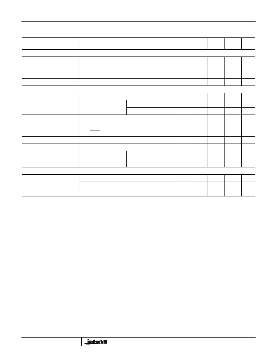
TRANSMITTER OUTPUTS
Output Voltage Swing
All Transmitter Outputs Loaded with 3k
to Ground
Full
±5.0
±5.4
-
V
Output Resistance
VCC = V+ = V- = 0V, Transmitter Output = ±2V
Full
300
10M
-
Output Short-Circuit Current
Shorted to GND
Full
-
±60
mA
Output Leakage Current
VOUT = ±12V, VCC = 0V or 3V to 5.5V, SHDN =GND
Full
-
±25
A
TIMING CHARACTERISTICS
Maximum Data Rate
RL =3k, CL = 1000pF, One Transmitter Switching
Full
250
500
-
kbps
Receiver Propagation Delay
Receiver Input to Receiver
Output, CL = 150pF
tPHL
25
-
0.15
-
s
tPLH
25
-
0.15
-
s
Receiver Output Enable Time
25
-
200
-
ns
Receiver Output Disable Time
25
-
200
-
ns
Transmitter Output Enable Time
From SHDN Rising Edge to TOUT = ±3.7V
25
-
100
-
s
Transmitter Skew
tPHL - tPLH (Note 2)
25
-
100
-
ns
Receiver Skew
tPHL - tPLH
25
-
50
-
ns
Transition Region Slew Rate
RL =3k to 7k,
Measured From 3V to -3V or
-3V to 3V, VCC = 3.3V
CL = 150pF to 1000pF
25
6
18
30
V/
s
CL = 150pF to 2500pF
25
4
13
30
V/
s
ESD PERFORMANCE
RS-232 Pins (TOUT, RIN)
Human Body Model
25
-
±15
-
kV
IEC61000-4-2 Air Gap Discharge
25
-
±15
-
kV
IEC61000-4-2 Contact Discharge
25
-
±8-
kV
NOTE:
2. Transmitter skew is measured at the transmitter zero crossing points.
Electrical Specifications
Test Conditions: VCC = 3V to 5.5V, C1 - C4 = 0.1F, VL = VCC; Unless Otherwise Specified.
Typicals are at TA = 25
oC, V
CC = VL = 3.3V (Continued)
PARAMETER
TEST CONDITIONS
TEMP
(oC)
MIN
TYP
MAX
UNITS
ISL83386E
相关PDF资料 |
PDF描述 |
|---|---|
| ISL83387EIV-T | IC 3DRVR/3RCVR RS232 3V 24-TSSOP |
| ISL83491IP | IC TXRX RS485/422 3.3V LP 14-DIP |
| ISL98002CRZ-170 | IC VID DIGITIZER 3CHN AFE 72-QFN |
| ISL98003CNZ-165 | IC AFE 3CH 8BIT 165MHZ 80EPTQFP |
| ISLA118P50IRZ | IC ADC 8BIT SPI/SRL 500M 72QFN |
相关代理商/技术参数 |
参数描述 |
|---|---|
| ISL83386EIVZ | 功能描述:RS-232接口集成电路 RS232 3V 3D/2R 15KV SHTDWN 20LD TSSOP RoHS:否 制造商:Exar 数据速率:52 Mbps 工作电源电压:5 V 电源电流:300 mA 工作温度范围:- 40 C to + 85 C 安装风格:SMD/SMT 封装 / 箱体:LQFP-100 封装: |
| ISL83386EIVZ-T | 功能描述:IC 3DRVR/2RCVR RS232 3V 20-TSSOP RoHS:是 类别:集成电路 (IC) >> 接口 - 驱动器,接收器,收发器 系列:- 标准包装:250 系列:- 类型:收发器 驱动器/接收器数:2/2 规程:RS232 电源电压:3 V ~ 5.5 V 安装类型:表面贴装 封装/外壳:16-TSSOP(0.173",4.40mm 宽) 供应商设备封装:16-TSSOP 包装:带卷 (TR) |
| ISL83387 | 制造商:INTERSIL 制造商全称:Intersil Corporation 功能描述:+/-15kV ESD Protected, +3V to +5.5V, 1Microamp, 250kbps, RS-232 Transceivers with Enhanced Automatic Powerdown and a Separate Logic Supply |
| ISL83387E | 制造商:INTERSIL 制造商全称:Intersil Corporation 功能描述:+/-15kV ESD Protected, +3V to +5.5V, 1Microamp, 250kbps, RS-232 Transceivers with Enhanced Automatic Powerdown and a Separate Logic Supply |
| ISL83387E_05 | 制造商:INTERSIL 制造商全称:Intersil Corporation 功能描述:+/-15kV ESD Protected, +3V to +5.5V, 1Microamp, 250kbps, RS-232 Transceivers with Enhanced Automatic Powerdown and a Separate Logic Supply |
发布紧急采购,3分钟左右您将得到回复。