- 您现在的位置:买卖IC网 > PDF目录15196 > ISL8843MBZ (Intersil)IC REG CTRLR BST FLYBK ISO 8SOIC PDF资料下载
参数资料
| 型号: | ISL8843MBZ |
| 厂商: | Intersil |
| 文件页数: | 9/12页 |
| 文件大小: | 0K |
| 描述: | IC REG CTRLR BST FLYBK ISO 8SOIC |
| 标准包装: | 980 |
| PWM 型: | 电流模式 |
| 输出数: | 1 |
| 频率 - 最大: | 2MHz |
| 占空比: | 100% |
| 电源电压: | 9 V ~ 30 V |
| 降压: | 是 |
| 升压: | 是 |
| 回扫: | 是 |
| 反相: | 无 |
| 倍增器: | 无 |
| 除法器: | 无 |
| Cuk: | 无 |
| 隔离: | 是 |
| 工作温度: | -55°C ~ 125°C |
| 封装/外壳: | 8-SOIC(0.154",3.90mm 宽) |
| 包装: | 管件 |
�� �
�
�ISL8843�
�Q� =� -------------------------------------------------�
�1�
�R� CS� =� ---------------------------------------------------------------------------------------------------------------------------------------------------------�
�D� ?� T� sw� ?� V� IN� ?� --� π� -� +� 0.5�
�?�
�(� 1� –� D� )� ?� V� O� ?� T� sw� ?�
�---------------------------------� ?� ?� ------------------� –� 1� ?� +� ------� s� -� ?� ?� I� O� +� ----------------------------------------------� ?�
�L� p�
�N� p� ?�
�2L� s�
�?� 1� –� D� ?�
�?� ?�
�frequency.� The� double-pole� will� be� critically� damped� if� the�
�Q-factor� is� set� to� 1,� over-damped� for� Q� <� 1,� and� under-�
�damped� for� Q� >� 1.� An� under-damped� condition� may� result� in�
�current� loop� instability.�
�(EQ.� 9)�
�π� (� m� c� (� 1� –� D� )� –� 0.5� )�
�Substituting� Equations� 12� and� 13� into� Equation� 14� and�
�solving� for� R� CS� yields�
�1�
�1�
�N� ?�
�?�
�(EQ.� 15)�
�where� D� is� the� percent� of� on� time� during� a� switching� cycle.�
�Setting� Q� =� 1� and� solving� for� Se� yields�
�Adding� slope� compensation� is� accomplished� in� the� ISL8843�
�S� e� =� S� n� ?� ?� ---� +� 0.5� ?� -------------� –� 1� ?�
�?� ?� π� ?� 1� –� D� ?�
�1� 1�
�(EQ.� 10)�
�using� an� external� buffer� transistor� and� the� RTCT� signal.� A�
�typical� application� sums� the� buffered� RTCT� signal� with� the�
�current� sense� feedback� and� applies� the� result� to� the� CS� pin�
�Since� Sn� and� Se� are� the� on� time� slopes� of� the� current� ramp�
�and� the� external� ramp,� respectively,� they� can� be� multiplied�
�by� Ton� to� obtain� the� voltage� change� that� occurs� during� Ton.�
�as� shown� in� Figure� 6.�
�V� e� =� V� n� ?� ?� 1� ---� +� 0.5� ?� -------------� –� 1� ?�
�?� ?� π� ?� 1� –� D� ?�
�1�
�(EQ.� 11)�
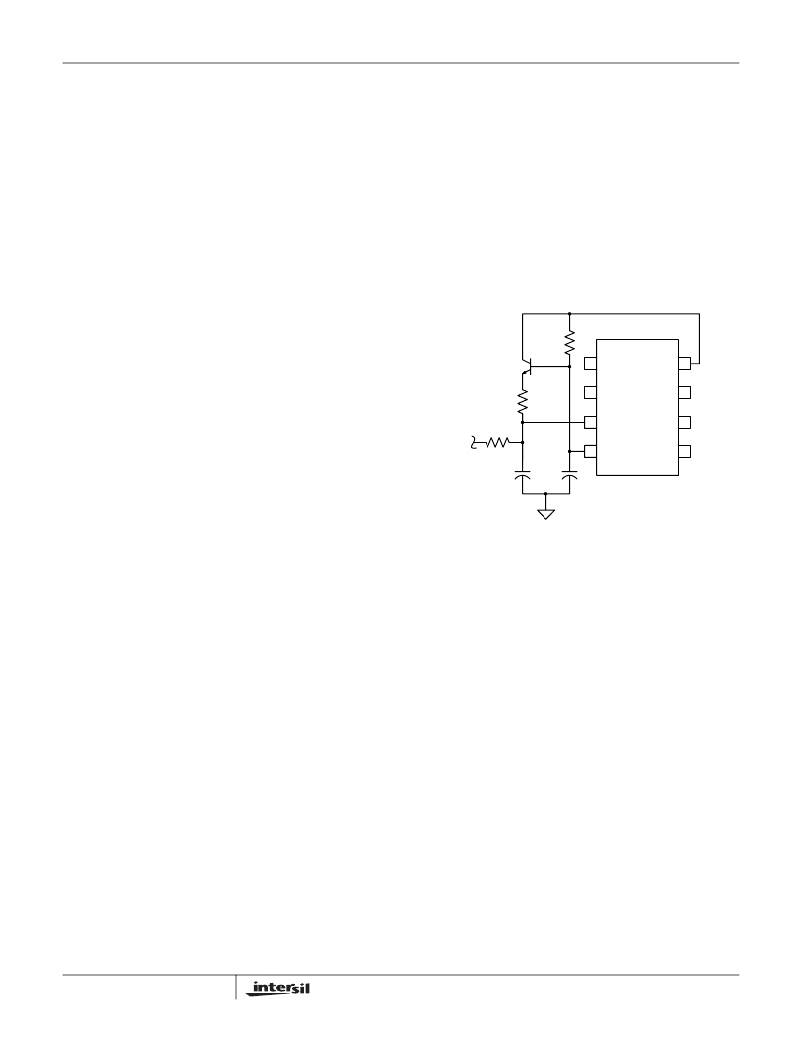
�VREF�
�where� Vn� is� the� change� in� the� current� feedback� signal� (� ?� I)�
�during� the� on� time� and� Ve� is� the� voltage� that� must� be� added�
�R9�
�by� the� external� ramp.�
�For� a� flyback� converter,� Vn� can� be� solved� for� in� terms� of�
�R6�
�CS�
�input� voltage,� current� transducer� components,� and� primary�
�inductance,� yielding�
�C4�
�RTCT�
�V� e� =� ----------------------------------------------------� ?� ?� ---� +� 0.5� ?� -------------� –� 1� ?�
�D� ?� T� SW� ?� V� IN� ?� R� CS� 1� 1�
�L� p� ?� ?� π� ?� 1� –� D� ?�
�V�
�(EQ.� 12)�
�FIGURE� 6.� SLOPE� COMPENSATION�
�where� R� CS� is� the� current� sense� resistor,� T� SW� is� the�
�switching� frequency,� L� p� is� the� primary� inductance,� V� IN� is� the�
�minimum� input� voltage,� and� D� is� the� maximum� duty� cycle.�
�The� current� sense� signal� at� the� end� of� the� ON� time� for� CCM�
�Assuming� the� designer� has� selected� values� for� the� RC� filter�
�(R6� and� C4)� placed� on� the� CS� pin,� the� value� of� R9� required�
�to� add� the� appropriate� external� ramp� can� be� found� by�
�superposition.�
�V� CS� =� ------------------------� ?� I� O� +� ----------------------------------------------� ?�
�V� e� =� ----------------------------� V�
�operation� is:�
�N� P� ?� 2L� s� ?�
�N� S� ?� R� CS� ?� (� 1� –� D� )� ?� V� O� ?� T� sw� ?�
�V�
�(EQ.� 13)�
�(EQ.� 16)�
�R6� +� R9�
�The� factor� of� 2.05� in� Equation� 16� arises� from� the� peak�
�amplitude� of� the� sawtooth� waveform� on� RTCT� minus� a� base-�
�where� V� CS� is� the� voltage� across� the� current� sense� resistor,�
�L� s� is� the� secondary� winding� inductance,� and� I� O� is� the� output�
�current� at� current� limit.� Equation� 13� assumes� the� voltage�
�emitter� junction� drop.� That� voltage� multiplied� by� the�
�maximum� duty� cycle� is� the� voltage� source� for� the� slope�
�compensation.� Rearranging� to� solve� for� R9� yields:�
�(� 2.05D� –� V� e� )� ?� R6�
�drop� across� the� output� rectifier� is� negligible.�
�Since� the� peak� current� limit� threshold� is� 1.00V,� the� total�
�current� feedback� signal� plus� the� external� ramp� voltage� must�
�R9� =� -----------------------------------------------�
�V� e�
�?�
�(EQ.� 17)�
�sum� to� this� value� when� the� output� load� is� at� the� current� limit�
�threshold.�
�The� value� of� R� CS� determined� in� Equation� 15� must� be�
�rescaled� so� that� the� current� sense� signal� presented� at� the�
�CS� pin� is� that� predicted� by� Equation� 13.� The� divider� created�
�V� e� +� V� CS� =� 1�
�(EQ.� 14)�
�by� R6� and� R9� makes� this� necessary.�
�R� ′� CS� =� ----------------------� ?� R� CS�
�9�
�R6� +� R9�
�R9�
�(EQ.� 18)�
�FN9238.1�
�January� 3,� 2006�
�相关PDF资料 |
PDF描述 |
|---|---|
| ACC17DREF | CONN EDGECARD 34POS .100 EYELET |
| VE-J4P-EW-F4 | CONVERTER MOD DC/DC 13.8V 100W |
| B41042A5108M | 1000UF 25V 12.5X25 SINGLE END |
| ISL8843AUZ | IC REG CTRLR BST FLYBK ISO 8MSOP |
| B41041A8108M | 1000UF 63V 16X31.5 SINGLE END |
相关代理商/技术参数 |
参数描述 |
|---|---|
| ISL8843MBZ-T | 功能描述:IC REG CTRLR BST FLYBK ISO 8SOIC RoHS:是 类别:集成电路 (IC) >> PMIC - 稳压器 - DC DC 切换控制器 系列:- 产品培训模块:Lead (SnPb) Finish for COTS Obsolescence Mitigation Program 标准包装:2,500 系列:- PWM 型:电流模式 输出数:1 频率 - 最大:275kHz 占空比:50% 电源电压:18 V ~ 110 V 降压:无 升压:无 回扫:无 反相:无 倍增器:无 除法器:无 Cuk:无 隔离:是 工作温度:-40°C ~ 85°C 封装/外壳:8-SOIC(0.154",3.90mm 宽) 包装:带卷 (TR) |
| ISL8843MUZ | 功能描述:IC REG CTRLR BST FLYBK ISO 8MSOP RoHS:是 类别:集成电路 (IC) >> PMIC - 稳压器 - DC DC 切换控制器 系列:- 产品培训模块:Lead (SnPb) Finish for COTS Obsolescence Mitigation Program 标准包装:2,500 系列:- PWM 型:电流模式 输出数:1 频率 - 最大:275kHz 占空比:50% 电源电压:18 V ~ 110 V 降压:无 升压:无 回扫:无 反相:无 倍增器:无 除法器:无 Cuk:无 隔离:是 工作温度:-40°C ~ 85°C 封装/外壳:8-SOIC(0.154",3.90mm 宽) 包装:带卷 (TR) |
| ISL8843MUZ-T | 功能描述:IC REG CTRLR BST FLYBK ISO 8MSOP RoHS:是 类别:集成电路 (IC) >> PMIC - 稳压器 - DC DC 切换控制器 系列:- 产品培训模块:Lead (SnPb) Finish for COTS Obsolescence Mitigation Program 标准包装:2,500 系列:- PWM 型:电流模式 输出数:1 频率 - 最大:275kHz 占空比:50% 电源电压:18 V ~ 110 V 降压:无 升压:无 回扫:无 反相:无 倍增器:无 除法器:无 Cuk:无 隔离:是 工作温度:-40°C ~ 85°C 封装/外壳:8-SOIC(0.154",3.90mm 宽) 包装:带卷 (TR) |
| ISL8844AABZ | 功能描述:IC REG CTRLR BST FLYBK ISO 8SOIC RoHS:是 类别:集成电路 (IC) >> PMIC - 稳压器 - DC DC 切换控制器 系列:- 产品培训模块:Lead (SnPb) Finish for COTS Obsolescence Mitigation Program 标准包装:2,500 系列:- PWM 型:电流模式 输出数:1 频率 - 最大:275kHz 占空比:50% 电源电压:18 V ~ 110 V 降压:无 升压:无 回扫:无 反相:无 倍增器:无 除法器:无 Cuk:无 隔离:是 工作温度:-40°C ~ 85°C 封装/外壳:8-SOIC(0.154",3.90mm 宽) 包装:带卷 (TR) |
| ISL8844AABZ-T | 功能描述:IC REG CTRLR BST FLYBK ISO 8SOIC RoHS:是 类别:集成电路 (IC) >> PMIC - 稳压器 - DC DC 切换控制器 系列:- 产品培训模块:Lead (SnPb) Finish for COTS Obsolescence Mitigation Program 标准包装:2,500 系列:- PWM 型:电流模式 输出数:1 频率 - 最大:275kHz 占空比:50% 电源电压:18 V ~ 110 V 降压:无 升压:无 回扫:无 反相:无 倍增器:无 除法器:无 Cuk:无 隔离:是 工作温度:-40°C ~ 85°C 封装/外壳:8-SOIC(0.154",3.90mm 宽) 包装:带卷 (TR) |
发布紧急采购,3分钟左右您将得到回复。