- 您现在的位置:买卖IC网 > Datasheet目录334 > ISL89162FBEBZ (Intersil)IC MOSFET DRIVER 2CH 6A 8SOIC Datasheet资料下载
参数资料
| 型号: | ISL89162FBEBZ |
| 厂商: | Intersil |
| 文件页数: | 10/14页 |
| 文件大小: | 0K |
| 描述: | IC MOSFET DRIVER 2CH 6A 8SOIC |
| 标准包装: | 980 |
| 配置: | 低端 |
| 输入类型: | 反相和非反相 |
| 延迟时间: | 25ns |
| 电流 - 峰: | 6A |
| 配置数: | 2 |
| 输出数: | 2 |
| 电源电压: | 4.5 V ~ 16 V |
| 工作温度: | -40°C ~ 125°C |
| 安装类型: | 表面贴装 |
| 封装/外壳: | 8-SOIC(0.154",3.90mm Width)裸露焊盘 |
| 供应商设备封装: | 8-SOIC-EP |
| 包装: | 管件 |
�� �
�
�ISL89160,� ISL89161,� ISL89162�
�Typical� Application� Circuit�
�V� BRIDGE�
�SQR�
�ZVS� FULL� BRIDGE�
�PWM�
�L�
�R�
�L�
�U1A�
�V� GUL�
�Q� UL�
�Q� UR�
�V� GUR�
�LL�
�SQR�
�ISL89162�
�LR�
�V� LL�
�U1B�
�T1A�
�T2�
�T1B�
�V� LR�
�Red� dashed� lines�
�emphasize� the�
�V� GLL�
�Q� LL�
�Q� LR�
�V� GLR�
�V� GLL�
�V� GUL�
�resonant� switching�
�delay� of� the� low-�
�side� bridge� FETs�
�LL�
�U2A�
�?� ISL89160�
�U2B�
�?� ISL89160�
�LR�
�LL:� Lower� Left�
�V� GLR�
�V� GUR�
�LR:� Lower� Right�
�UL:� Upper� Left�
�UR:� Upper� Right�
�GLL:� Gate� Lower� Left�
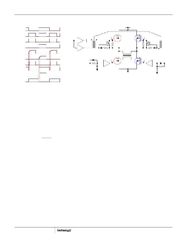
�This� is� an� example� of� how� the� ISL89160,� ISL89161,� ISL89162,�
�MOSFET� drivers� can� be� applied� in� a� zero� voltage� switching� full�
�bridge.� Two� main� signals� are� required:� a� 50%� duty� cycle� square�
�wave� (SQR)� and� a� PWM� signal� synchronized� to� the� edges� of� the�
�SQR� input.� An� ISL89162� is� used� to� drive� T1� with� alternating� half�
�cycles� driving� Q� UL� and� Q� UR� .� An� ISL89160� is� used� to� drive� Q� LL� and�
�Q� LR� also� with� alternating� half� cycles.� Unlike� the� two� high-side�
�bridge� FETs,� the� two� low� side� bridge� FETs� are� turned� on� with� a�
�rising� edge� delay.� The� delay� is� setup� by� the� RCD� network� on� the�
�inputs� to� the� ISL89160.� The� duration� of� the� delay� is� chosen� to�
�turn� on� the� low-side� FETs� when� the� voltage� on� their� respective�
�drains� is� at� the� resonant� valley.� For� a� complete� description� of� the�
�ZVS� topology,� refer� to� AN1603� “ISL6752_54� Evaluation� Board�
�Application� Note”.�
�General� PCB� Layout� Guidelines�
�The� AC� performance� of� the� ISL89160,� ISL89161,� ISL89162�
�depends� significantly� on� the� design� of� the� PC� board.� The�
�following� layout� design� guidelines� are� recommended� to� achieve�
�optimum� performance:�
�?� Place� the� driver� as� close� as� possible� to� the� driven� power� FET.�
�?� Understand� where� the� switching� power� currents� flow.� The� high�
�amplitude� di/dt� currents� of� the� driven� power� FET� will� induce�
�significant� voltage� transients� on� the� associated� traces.�
�?� Keep� power� loops� as� short� as� possible� by� paralleling� the�
�source� and� return� traces.�
�?� Use� planes� where� practical;� they� are� usually� more� effective�
�than� parallel� traces.�
�?� Avoid� paralleling� high� amplitude� di/dt� traces� with� low� level�
�signal� lines.� High� di/dt� will� induce� currents� and� consequently,�
�noise� voltages� in� the� low� level� signal� lines.�
�?� When� practical,� minimize� impedances� in� low� level� signal�
�circuits.� The� noise,� magnetically� induced� on� a� 10k� resistor,� is�
�10x� larger� than� the� noise� on� a� 1k� resistor.�
�10�
�?� Be� aware� of� magnetic� fields� emanating� from� transformers� and�
�inductors.� Gaps� in� these� structures� are� especially� bad� for�
�emitting� flux.�
�?� If� you� must� have� traces� close� to� magnetic� devices,� align� the�
�traces� so� that� they� are� parallel� to� the� flux� lines� to� minimize�
�coupling.�
�?� The� use� of� low� inductance� components� such� as� chip� resistors�
�and� chip� capacitors� is� highly� recommended.�
�?� Use� decoupling� capacitors� to� reduce� the� influence� of� parasitic�
�inductance� in� the� VDD� and� GND� leads.� To� be� effective,� these�
�caps� must� also� have� the� shortest� possible� conduction� paths.� If�
�vias� are� used,� connect� several� paralleled� vias� to� reduce� the�
�inductance� of� the� vias.�
�?� It� may� be� necessary� to� add� resistance� to� dampen� resonating�
�parasitic� circuits� especially� on� OUTA� and� OUTB.� If� an� external�
�gate� resistor� is� unacceptable,� then� the� layout� must� be�
�improved� to� minimize� lead� inductance.�
�?� Keep� high� dv/dt� nodes� away� from� low� level� circuits.� Guard�
�banding� can� be� used� to� shunt� away� dv/dt� injected� currents�
�from� sensitive� circuits.� This� is� especially� true� for� control� circuits�
�that� source� the� input� signals� to� the� ISL89160,� ISL89161,�
�ISL89162.�
�?� Avoid� having� a� signal� ground� plane� under� a� high� amplitude�
�dv/dt� circuit.� This� will� inject� di/dt� currents� into� the� signal�
�ground� paths.�
�?� Do� power� dissipation� and� voltage� drop� calculations� of� the�
�power� traces.� Many� PCB/CAD� programs� have� built� in� tools� for�
�calculation� of� trace� resistance.�
�?� Large� power� components� (Power� FETs,� Electrolytic� caps,� power�
�resistors,� etc.)� will� have� internal� parasitic� inductance� which�
�cannot� be� eliminated.� This� must� be� accounted� for� in� the� PCB�
�layout� and� circuit� design.�
�?� If� you� simulate� your� circuits,� consider� including� parasitic�
�components� especially� parasitic� inductance.�
�FN7719.3�
�February� 20,� 2013�
�相关PDF资料 |
PDF描述 |
|---|---|
| ISL89165FBECZ | MOSFET DRIVER 2CH 6A 8SOIC |
| ISL89168FBEAZ | IC MOSFET DRIVER 2CH 6A 8SOIC |
| ISL89367FRTAZ | IC MOSFET DRIVER 2CH 6A 16TDFN |
| ISL89401ABZ | IC DRVR H-BRDG 100V 1.25A 8SOIC |
| ISL89410IBZ-T13 | IC DRVR MOSFET DUAL-CH 8-SOIC |
相关代理商/技术参数 |
参数描述 |
|---|---|
| ISL89162FBEBZ-T | 功能描述:IC MOSFET DRIVER 2CH 6A 8SOIC RoHS:是 类别:集成电路 (IC) >> PMIC - MOSFET,电桥驱动器 - 外部开关 系列:- 标准包装:6,000 系列:* |
| ISL89162FRTAZ | 功能描述:IC MOSFET DRIVER 2CH 6A 8TDFN RoHS:是 类别:集成电路 (IC) >> PMIC - MOSFET,电桥驱动器 - 外部开关 系列:- 标准包装:6,000 系列:* |
| ISL89162FRTAZ-T | 功能描述:IC MOSFET DRIVER 2CH 6A 8TDFN RoHS:是 类别:集成电路 (IC) >> PMIC - MOSFET,电桥驱动器 - 外部开关 系列:- 标准包装:6,000 系列:* |
| ISL89162FRTBZ | 功能描述:IC MOSFET DRIVER 2CH 6A 8TDFN RoHS:是 类别:集成电路 (IC) >> PMIC - MOSFET,电桥驱动器 - 外部开关 系列:- 标准包装:6,000 系列:* |
| ISL89162FRTBZ-T | 功能描述:IC MOSFET DRIVER 2CH 6A 8TDFN RoHS:是 类别:集成电路 (IC) >> PMIC - MOSFET,电桥驱动器 - 外部开关 系列:- 标准包装:6,000 系列:* |
发布紧急采购,3分钟左右您将得到回复。