参数资料
| 型号: | ISL90726WIE627Z-TK |
| 厂商: | Intersil |
| 文件页数: | 6/8页 |
| 文件大小: | 0K |
| 描述: | IC POT DGTL 10K OHM SC70-6 |
| 产品培训模块: | Digitally Controlled Potentiometers Solutions for Industrial Control Applications |
| 标准包装: | 1 |
| 系列: | XDCP™ |
| 接片: | 128 |
| 电阻(欧姆): | 10k |
| 电路数: | 1 |
| 温度系数: | 标准值 ±45 ppm/°C |
| 存储器类型: | 易失 |
| 接口: | I²C |
| 电源电压: | 2.7 V ~ 5.5 V |
| 工作温度: | -40°C ~ 85°C |
| 安装类型: | 表面贴装 |
| 封装/外壳: | 6-TSSOP,SC-88,SOT-363 |
| 供应商设备封装: | SC-70-6 |
| 包装: | 标准包装 |
| 产品目录页面: | 1237 (CN2011-ZH PDF) |
| 其它名称: | ISL90726WIE627Z-TKDKR |
6
FN8244.4
August 26, 2008
I2C Serial Interface
The ISL90726 supports bidirectional bus oriented protocol.
The protocol defines any device that sends data onto the
bus as a transmitter and the receiving device as the receiver.
The device controlling the transfer is a master and the
device being controlled is the slave. The master always
initiates data transfers and provides the clock for both
transmit and receive operations. Therefore, the ISL90726
operates as slave device in all applications.
All communication over the I2C interface is conducted by
sending the MSB of each byte of data first.
Protocol Conventions
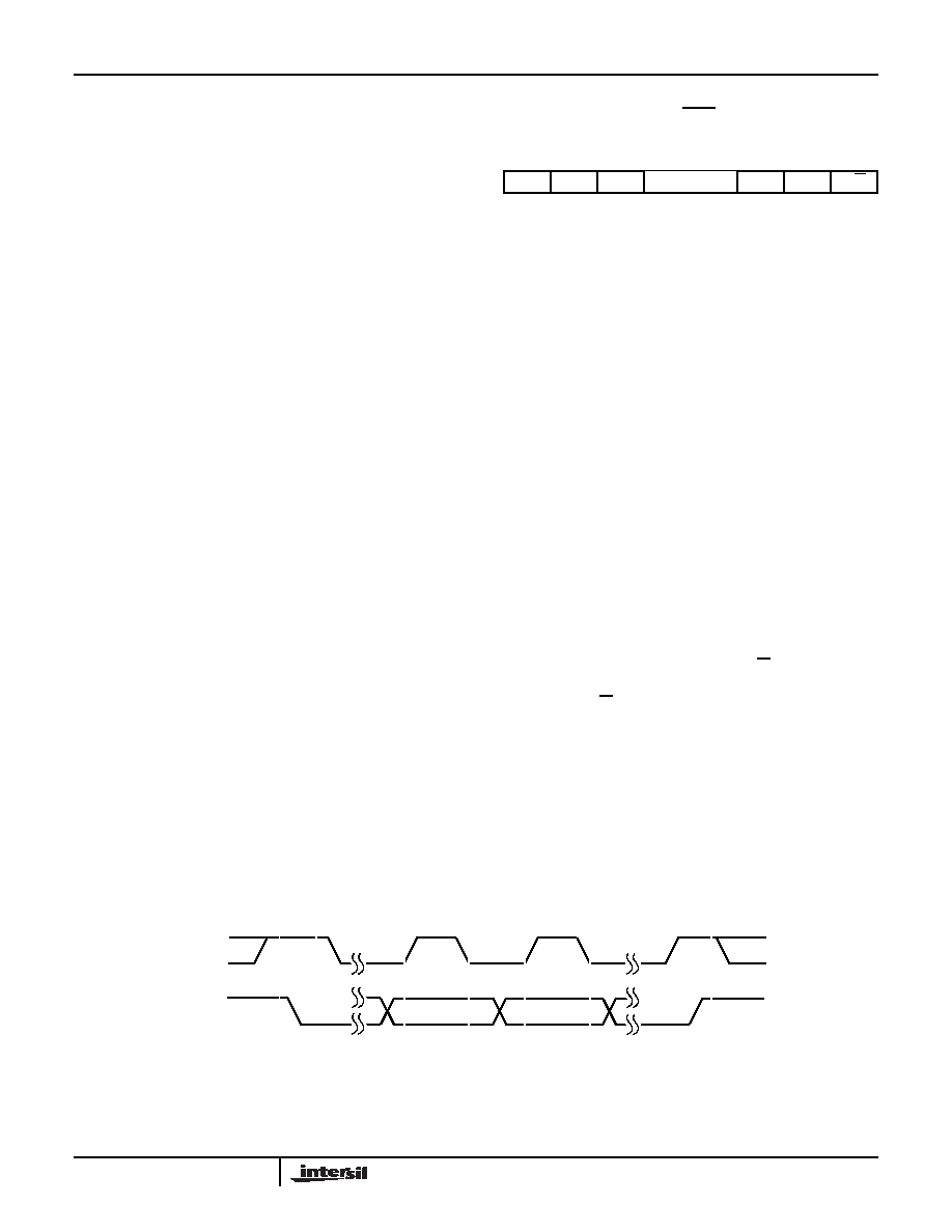
Data states on the SDA line can change only during SCL
LOW periods. SDA state changes during SCL HIGH are
reserved for indicating START and STOP conditions (see
Figure 1). On power-up of the ISL90726, the SDA pin is in
the input mode.
All I2C interface operations must begin with a START
condition, which is a HIGH to LOW transition of SDA while
SCL is HIGH. The ISL90726 continuously monitors the SDA
and SCL lines for the START condition and does not
respond to any command until this condition is met (see
Figure 1). A START condition is ignored during the power-up
sequence and during internal non-volatile write cycles.
All I2C interface operations must be terminated by a STOP
condition, which is a LOW to HIGH transition of SDA while
SCL is HIGH (see Figure 1).
An ACK, Acknowledge, is a software convention used to
indicate a successful data transfer. The transmitting device,
either master or slave, releases the SDA bus after
transmitting eight bits. During the ninth clock cycle, the
receiver pulls the SDA line LOW to acknowledge the
reception of the eight bits of data (see Figure 2).
The ISL90726 responds with an ACK after recognition of a
START condition followed by a valid Identification Byte, and
once again after successful receipt of an Address Byte. The
ISL90726 also responds with an ACK after receiving a Data
Byte of a write operation. The master must respond with an
ACK after receiving a Data Byte of a read operation.
A valid Identification Byte contains 0101110 as the seven
MSBs. The LSB in the Read/Write bit. Its value is “1” for a
Read operation, and “0” for a Write operation (see Table 1).
Write Operation
A Write operation requires a START condition, followed by a
valid Identification Byte, a valid Address Byte, a Data Byte,
and a STOP condition. After each of the three bytes, the
ISL90726 responds with an ACK. At this time, the device
enters its standby state (see Figure 3).
Data Protection
A valid Identification Byte, Address Byte, and total number of
SCL pulses act as a protection of both volatile and non-
volatile registers. During a Write sequence, the Data Byte is
loaded into an internal shift register as it is received. If the
Address Byte is 0h, the Data Byte is transferred to the Wiper
Register (WR) at the falling edge of the SCL pulse that loads
the last bit (LSB) of the Data Byte. If an address other than
00h, or an invalid slave address is sent, then the device will
respond with no ACK.
Read Operation
A Read operation consist of a three byte instruction followed
by one or more Data Bytes (see Figure 4). The master
initiates the operation issuing the following sequence: a
START, the Identification byte with the R/W bit set to “0”, an
Address Byte, a second START, and a second Identification
byte with the R/W bit set to “1”. After each of the three bytes,
the ISL90726 responds with an ACK. Then the ISL90726
transmits the Data Byte as long as the master responds with
an ACK during the SCL cycle following the eighth bit of each
byte. The master then terminates the read operation (issuing
a STOP condition) following the last bit of the Data Byte
(see Figure 4).
TABLE 1. IDENTIFICATION BYTE FORMAT
0101110
R/W
(MSB)
(LSB)
SDA
SCL
START
DATA
STOP
STABLE
CHANGE
DATA
STABLE
FIGURE 1. VALID DATA CHANGES, START, AND STOP CONDITIONS
ISL90726
相关PDF资料 |
PDF描述 |
|---|---|
| MS27656E17B6P | CONN RCPT 6POS WALL MNT W/PINS |
| VI-23L-MY-F1 | CONVERTER MOD DC/DC 28V 50W |
| VI-23K-MY-F4 | CONVERTER MOD DC/DC 40V 50W |
| VI-23K-MY-F2 | CONVERTER MOD DC/DC 40V 50W |
| MS3100A36-7P | CONN RCPT 47POS WALL MNT W/PINS |
相关代理商/技术参数 |
参数描述 |
|---|---|
| ISL90726WIE6Z | 制造商:INTERSIL 制造商全称:Intersil Corporation 功能描述:Digitally Controlled Potentiometer (XDCP) |
| ISL90726WIE6Z-TK | 制造商:INTERSIL 制造商全称:Intersil Corporation 功能描述:Digitally Controlled Potentiometer (XDCP) |
| ISL90727 | 制造商:INTERSIL 制造商全称:Intersil Corporation 功能描述:Digitally Controlled Potentiometer XDCP |
| ISL90727_06 | 制造商:INTERSIL 制造商全称:Intersil Corporation 功能描述:Digitally Controlled Potentiometer |
| ISL90727UIE627Z | 功能描述:IC XDCP 128-TAP 50KOHM SC70-6 RoHS:是 类别:集成电路 (IC) >> 数据采集 - 数字电位器 系列:XDCP™ 标准包装:2,500 系列:XDCP™ 接片:256 电阻(欧姆):100k 电路数:1 温度系数:标准值 ±300 ppm/°C 存储器类型:非易失 接口:I²C(设备位址) 电源电压:2.7 V ~ 5.5 V 工作温度:0°C ~ 70°C 安装类型:表面贴装 封装/外壳:14-TSSOP(0.173",4.40mm 宽) 供应商设备封装:14-TSSOP 包装:带卷 (TR) |
发布紧急采购,3分钟左右您将得到回复。