参数资料
| 型号: | ISL90840WIV2027ZT2 |
| 厂商: | Intersil |
| 文件页数: | 2/13页 |
| 文件大小: | 0K |
| 描述: | IC XDCP 256-TAP 10KOHM TSSOP-20 |
| 标准包装: | 2,500 |
| 系列: | XDCP™ |
| 接片: | 256 |
| 电阻(欧姆): | 10k |
| 电路数: | 4 |
| 温度系数: | 标准值 ±45 ppm/°C |
| 存储器类型: | 易失 |
| 接口: | I²C(设备位址) |
| 电源电压: | 2.7 V ~ 5.5 V |
| 工作温度: | -40°C ~ 85°C |
| 安装类型: | 表面贴装 |
| 封装/外壳: | 20-TSSOP(0.173",4.40mm 宽) |
| 供应商设备封装: | 20-TSSOP |
| 包装: | 带卷 (TR) |
10
FN8086.2
November 14, 2006
Principles of Operation
The ISL90840 is an integrated circuit incorporating four
DCPs with their associated registers, and an I2C serial
interface providing direct communication between a host
and the potentiometers.
DCP Description
Each DCP is implemented with a combination of resistor
elements and CMOS switches. The physical ends of each
DCP are equivalent to the fixed terminals of a mechanical
potentiometer (RH and RL pins). The RW pin of each DCP is
connected to intermediate nodes, and is equivalent to the
wiper terminal of a mechanical potentiometer. The position
of the wiper terminal within the DCP is controlled by an 8-bit
volatile Wiper Register (WR). Each DCP has its own WR.
When the WR of a DCP contains all zeroes (WR[7:0]: 00h),
its wiper terminal (RW) is closest to its “Low” terminal (RL).
When the WR of a DCP contains all ones (WR[7:0]: FFh), its
wiper terminal (RW) is closest to its “High” terminal (RH). As
the value of the WR increases from all zeroes (0 decimal) to
all ones (255 decimal), the wiper moves monotonically from
the position closest to RL to the closest to RH. At the same
time, the resistance between RW and RL increases
monotonically, while the resistance between RH and RW
decreases monotonically.
While the ISL90840 is being powered up, all four WRs are
reset to 80h (128 decimal), which locates RW roughly at the
center between RL and RH.
The WRs can be read or written to directly using the I2C
serial interface as described in the following sections. The
I2C interface Address Byte has to be set to 00h, 01h, 02h,
and 03h to access the WR of DCP0, DCP1, DCP2, and
DCP3 respectively
I2C Serial Interface
The ISL90840 supports a bidirectional bus oriented protocol.
The protocol defines any device that sends data onto the
bus as a transmitter and the receiving device as the receiver.
The device controlling the transfer is a master and the
device being controlled is the slave. The master always
initiates data transfers and provides the clock for both
transmit and receive operations. Therefore, the ISL90840
operates as a slave device in all applications.
All communication over the I2C interface is conducted by
sending the MSB of each byte of data first.
Protocol Conventions
Data states on the SDA line must change only during SCL
LOW periods. SDA state changes during SCL HIGH are
reserved for indicating START and STOP conditions (See
Figure 15). On power-up of the ISL90840 the SDA pin is in
the input mode.
All I2C interface operations must begin with a START
condition, which is a HIGH to LOW transition of SDA while
SCL is HIGH. The ISL90840 continuously monitors the SDA
and SCL lines for the START condition and does not
respond to any command until this condition is met (See
Figure 15). A START condition is ignored during the power-
up of the device.
All I2C interface operations must be terminated by a STOP
condition, which is a LOW to HIGH transition of SDA while
SCL is HIGH (See Figure 15). A STOP condition at the end
of a read operation, or at the end of a write operation places
the device in its standby mode.
An acknowledge (ACK) is a software convention used to
indicate a successful data transfer. The transmitting device,
either master or slave, releases the SDA bus after
transmitting eight bits. During the ninth clock cycle, the
receiver pulls the SDA line LOW to acknowledge the
reception of the eight bits of data (See Figure 16).
The ISL90840 responds with an ACK after recognition of a
START condition followed by a valid Identification Byte, and
once again after successful receipt of an Address Byte. The
ISL90840 also responds with an ACK after receiving a Data
Byte of a write operation. The master must respond with an
ACK after receiving a Data Byte of a read operation
A valid Identification Byte contains 0101 as the four MSBs,
and the following three bits matching the logic values
present at pins A2, A1, and A0. The LSB is the Read/Write
bit. Its value is “1” for a Read operation, and “0” for a Write
operation (See Table 1).
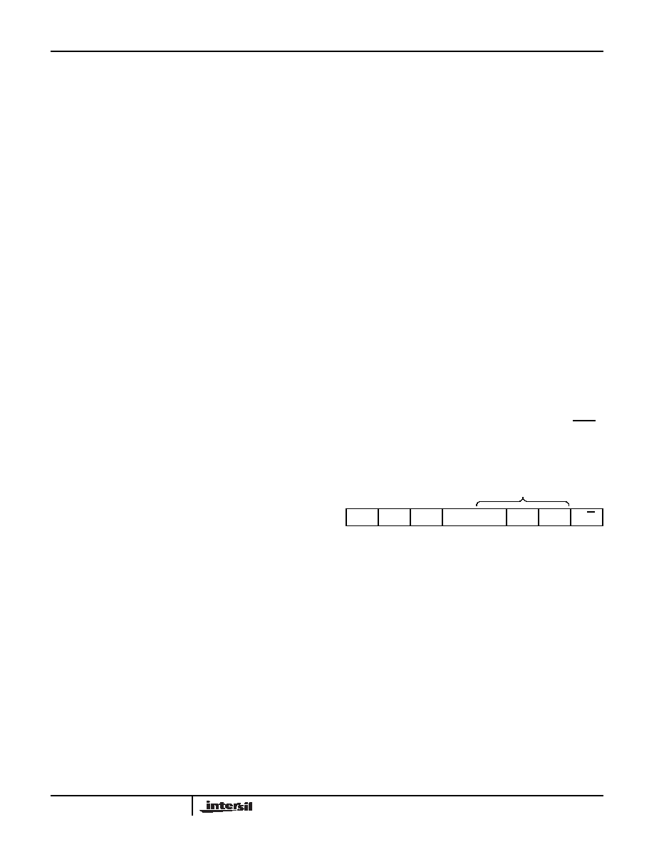
TABLE 1. IDENTIFICATION BYTE FORMAT
0101
A2
A1
A0
R/W
(MSB)
(LSB)
Logic values at pins A2, A1, and A0 respectively
ISL90840
相关PDF资料 |
PDF描述 |
|---|---|
| ISL90841WIV1427Z | IC XDCP 256-TAP 10KOHM TSSOP-14 |
| ISL90842UIV1427Z | IC DCP 256-TAP 50KOHM TSSOP-14 |
| ISL90843UIU1027Z-TK | IC XDCP 256-TAP 50OHM 10-MSOP |
| ISL95310WIU10Z | IC XDCP 128-TAP 10KOHM 10-MSOP |
| ISL95311WIU10Z | IC XDCP 128-TAP 10KOHM 10-MSOP |
相关代理商/技术参数 |
参数描述 |
|---|---|
| ISL90841 | 制造商:INTERSIL 制造商全称:Intersil Corporation 功能描述:Low Noise, Low Power I2C Bus, 256 Taps |
| ISL90841_06 | 制造商:INTERSIL 制造商全称:Intersil Corporation 功能描述:Quad Digitally Controlled Potentiometers (XDCP⑩) |
| ISL90841UIV1427 | 制造商:INTERSIL 制造商全称:Intersil Corporation 功能描述:Low Noise, Low Power I2C Bus, 256 Taps |
| ISL90841UIV1427Z | 功能描述:IC XDCP 256-TAP 50KOHM TSSOP-14 RoHS:是 类别:集成电路 (IC) >> 数据采集 - 数字电位器 系列:XDCP™ 产品培训模块:Lead (SnPb) Finish for COTS Obsolescence Mitigation Program 标准包装:2,500 系列:- 接片:256 电阻(欧姆):100k 电路数:2 温度系数:标准值 35 ppm/°C 存储器类型:易失 接口:6 线串行(芯片选择,递增,增/减) 电源电压:2.6 V ~ 5.5 V 工作温度:-40°C ~ 125°C 安装类型:表面贴装 封装/外壳:14-TSSOP(0.173",4.40mm 宽) 供应商设备封装:14-TSSOP 包装:带卷 (TR) |
| ISL90841UIV1427Z-TK | 功能描述:IC POT DGTL QUAD 50K OHM 14TSSOP RoHS:是 类别:集成电路 (IC) >> 数据采集 - 数字电位器 系列:XDCP™ 产品培训模块:Lead (SnPb) Finish for COTS Obsolescence Mitigation Program 标准包装:2,500 系列:- 接片:256 电阻(欧姆):100k 电路数:2 温度系数:标准值 35 ppm/°C 存储器类型:易失 接口:6 线串行(芯片选择,递增,增/减) 电源电压:2.6 V ~ 5.5 V 工作温度:-40°C ~ 125°C 安装类型:表面贴装 封装/外壳:14-TSSOP(0.173",4.40mm 宽) 供应商设备封装:14-TSSOP 包装:带卷 (TR) |
发布紧急采购,3分钟左右您将得到回复。