- 您现在的位置:买卖IC网 > PDF目录16590 > ISL97652IRZ-TK (Intersil)IC LCD SUPPLY 4CH DUAL AMP 48QFN PDF资料下载
参数资料
| 型号: | ISL97652IRZ-TK |
| 厂商: | Intersil |
| 文件页数: | 13/25页 |
| 文件大小: | 0K |
| 描述: | IC LCD SUPPLY 4CH DUAL AMP 48QFN |
| 标准包装: | 1,000 |
| 应用: | LCD 电视机/监控器 |
| 电流 - 电源: | 500µA |
| 电源电压: | 8 V ~ 15 V |
| 工作温度: | -40°C ~ 85°C |
| 安装类型: | 表面贴装 |
| 封装/外壳: | 48-VFQFN 裸露焊盘 |
| 供应商设备封装: | 48-QFN(7x7) |
| 包装: | 带卷 (TR) |
�� �
�
�ISL97652�
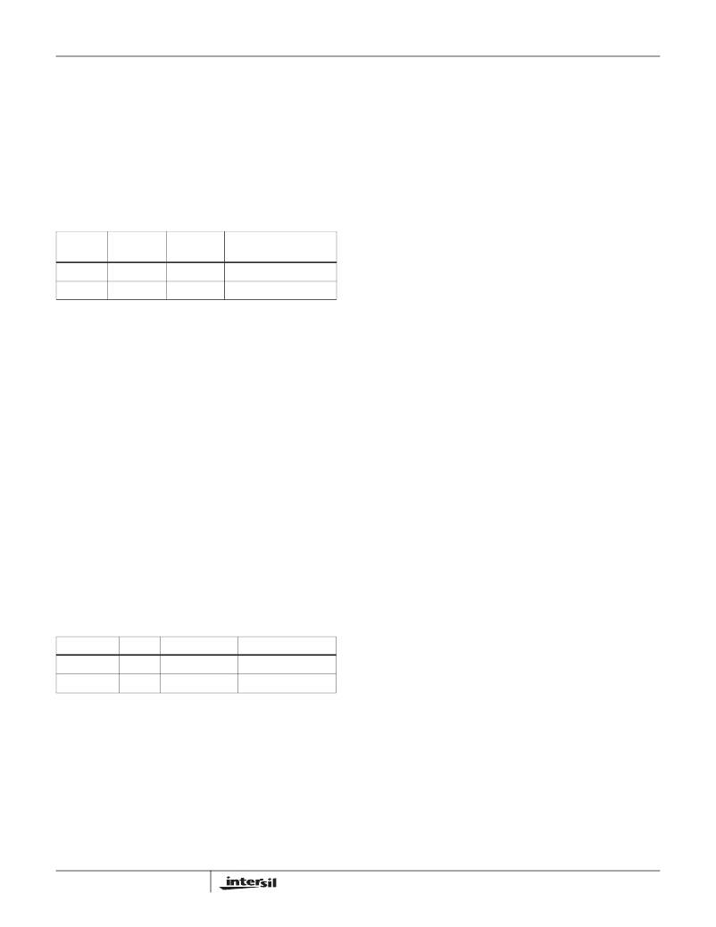
�Rectifier� Diode� (Boost� Converter)�
�A� high-speed� diode� is� necessary� due� to� the� high� switching�
�frequency.� Schottky� diodes� are� recommended� because� of�
�their� fast� recovery� time� and� low� forward� voltage.� The� reverse�
�voltage� rating� of� this� diode� should� be� higher� than� the�
�maximum� output� voltage.� The� rectifier� diode� must� meet� the�
�output� current� and� peak� inductor� current� requirements.� The�
�following� table� is� some� recommendations� for� boost� converter�
�diode.�
�TABLE� 4.� BOOST� CONVERTER� RECTIFIER� DIODE�
�RECOMMENDATION�
�examined� with� an� oscilloscope� set� to� AC� 100mV/div� and� the�
�amount� of� ringing� observed� when� the� load� current� changes.�
�Reduce� excessive� ringing� by� reducing� the� value� of� the�
�resistor� in� series� with� the� VC� pin� capacitor.�
�A� VDD� Delay� Switch�
�The� ISL97652� integrates� a� PMOS� disconnect� switch� for� the�
�A� VDD� boost� output� to� disconnect� V� IN� from� A� VDD� when� the�
�EN2� input� is� not� selected.� When� EN2� is� taken� high,� the�
�PMOS� FET� is� turned� on� to� connect� power� to� the� display.� The�
�CSUI� capacitor� provide� soft-start� control� for� the� connection�
�of� this� switch.�
�DIODE�
�SS23�
�SL23�
�V� R� /I� AVG�
�RATING�
�30V/2A�
�30V/2A�
�PACKAGE�
�SMB�
�SMB�
�VENDOR�
�Fairchild� Semiconductor�
�Vishay� Semiconductor�
�The� operation� of� the� AVDD� delay� switch� is� controlled� by�
�internal� VDSOK� and� VDSHYS� control� signals� which� operate�
�as� follows:�
�During� start-up� (or� during� fault� conditions):�
�VDSOK� goes� to� 1� when� V(SWI� -� SWO)� becomes� less� than�
�Output� Capacitor�
�The� output� capacitor� supplies� the� load� directly� and� reduces�
�the� ripple� voltage� at� the� output.� Output� ripple� voltage� consists�
�of� two� components:� the� voltage� drop� due� to� the� inductor� ripple�
�current� flowing� through� the� ESR� of� output� capacitor,� and� the�
�charging� and� discharging� of� the� output� capacitor.�
�~0.5V.� This� will� turn-on� the� boost� function.�
�VDSOK� goes� to� 0� when� VDS_pfet� becomes� greater� than�
�~1.1V.� This� will� turn-off� the� boost� function.�
�The� threshold� voltages� have� a� Vin� dependence� such� that:�
�For� Vin1� =� 8V:� VDSOK� goes� to� 1� occurs� at� ~0.5V� and�
�VDSOK� goes� to� 0� occurs� at� ~1.1V.�
�V� RIPPLE� =� I� LPK� � ESR� +� ------------------------� � --------------------� � ----�
�V� C� f�
�O� AVDD� s�
�V� O� –� V� IN� I� O� 1�
�(EQ.� 7)�
�For� Vin1� =18.5V:� VDSOK� goes� to1� occurs� at� ~1.13V� and�
�VDSOK� goes� to� 0� occurs� at� ~2.65V.�
�For� low� ESR� ceramic� capacitors,� the� output� ripple� is�
�dominated� by� the� charging� and� discharging� of� the� output�
�capacitor.� The� voltage� rating� of� the� output� capacitor� should�
�be� greater� than� the� maximum� output� voltage.�
�Note:� Capacitors� have� a� voltage� coefficient� that� makes� their�
�effective� capacitance� drop� as� the� voltage� across� then�
�increases.� C� OUT� in� Equation� 7� above� assumes� the� effective�
�value� of� the� capacitor� at� a� particular� voltage� and� not� the�
�manufacturer's� stated� value,� measured� at� zero� volts.�
�The� following� table� shows� some� selections� of� output�
�capacitors.�
�TABLE� 5.� BOOST� OUTPUT� CAPACITOR� RECOMMENDATION�
�V(SWI� -� SWO)� is� the� VDS� voltage� across� the� internal� PFET�
�protection� switch.� If� this� voltage� exceeds� 1.1V� for� some�
�reason� (e.g.� under� fault� conditions� or� during� start-up� if�
�VMAIN� rises� faster� than� AVDD)� the� boost� is� turned-off� to�
�allow� the� AVDD� (SWO)� potential� to� catch-up� with� VMAIN�
�(SWI).�
�VDSHYS� is� the� VDS� hysteresis� level;�
�Once� VDSOK� goes� to� 1� the� voltage� V(SWI� -� SWO)� then�
�needs� to� exceed� 1.1V� for� VDSOK� goes� to� 0.�
�During� normal� operation� VDS� will� be� ~Ron_PFET� *� Iload�
�(~� 0.18x2� =� 0.36V� for� max� AVDD� load).�
�If� a� fault� develops� on� AVDD,� which� causes� VDS� to� exceed�
�1.1V,� then� the� boost� operation� is� interrupted� by� the� internal�
�CAPACITOR�
�10μF/25V�
�10μF/25V�
�SIZE�
�1210�
�1210�
�VENDOR�
�TDK�
�Murata�
�PART� NUMBER�
�C3225X7R1E106M�
�GRM32DR61E106K�
�VDSOK� goes� to� 0� signal� and� fault� timers� will� start� to� operate�
�while� the� rising/falling� character� of� AVDD� is� monitored.�
�A� VDD� Delay� Switch� Fault� Operation�
�When� enabled,� the� gate� of� the� PFET� is� pulled� down� with� a�
�Loop� Compensation� (Boost� Converter)�
�The� boost� converter� of� ISL97652� can� be� compensated� by� a�
�RC� network� connected� from� V� C� pin� to� ground.� C� C� =� 4.7nF�
�and� R� C� =� 10k� RC� network� is� used� in� the� demo� board.� A�
�higher� resistor� value� can� be� used� to� lower� the� transient� load�
�change� A� VDD� overshoot� -� however,� this� may� be� at� the�
�expense� of� stability� to� the� loop.�
�The� stability� can� be� examined� by� repeatedly� changing� the�
�load� between� 100mA� and� a� max� level� that� is� likely� to� be�
�used� in� the� system� being� used.� The� A� VDD� voltage� should� be�
�13�
�30μA� current,� turning� on� the� FET� switch.� The� speed� of� this�
�turn-on� can� be� controlled� by� placing� a� capacitor� from� SWI� to�
�SUI.� In� normal� operation� the� gate� (and� SUI� pin)� are� pulled�
�down� to� 5V� below� SWI.� The� A� VDD� delay� switch� circuitry�
�constantly� monitors� both� the� current� in� the� switch� and� the�
�voltage� at� SWO.� If� the� current� exceeds� the� current� limit� of�
�2A,� the� gate� of� the� FET� (and� also� the� SUI� pin)� will� be� pulled�
�up� to� the� correct� level� to� limit� the� current� to� 2A.� In� this� mode�
�the� switch� acts� like� a� 2A� current� source.� this� current� cannot�
�be� maintained� indefinitely� due� to� the� power� dissipation� on�
�FN9287.1�
�November� 2,� 2007�
�相关PDF资料 |
PDF描述 |
|---|---|
| H3DWH-3418G | IDC CABLE - HKR34H/AE34G/HPL34H |
| ISL97652IRZ-T | IC LCD SUPPLY 4CH DUAL AMP 48QFN |
| H3DKH-3418G | IDC CABLE - HKR34H/AE34G/HPK34H |
| AK670M/2-2-GR-R | CABLE USB A-MINI B 4PIN V2.0 2M |
| EEM15DSEF | CONN EDGECARD 30POS .156 EYELET |
相关代理商/技术参数 |
参数描述 |
|---|---|
| ISL97653AIRZ | 功能描述:电流型 PWM 控制器 5-CH INTEGRTD LCD SUPPLY W/TEMP SENSOR RoHS:否 制造商:Texas Instruments 开关频率:27 KHz 上升时间: 下降时间: 工作电源电压:6 V to 15 V 工作电源电流:1.5 mA 输出端数量:1 最大工作温度:+ 105 C 安装风格:SMD/SMT 封装 / 箱体:TSSOP-14 |
| ISL97653AIRZ-T | 功能描述:电流型 PWM 控制器 5-CH INTEGRTD LCD SUPPLY W/TEMP SENSOR RoHS:否 制造商:Texas Instruments 开关频率:27 KHz 上升时间: 下降时间: 工作电源电压:6 V to 15 V 工作电源电流:1.5 mA 输出端数量:1 最大工作温度:+ 105 C 安装风格:SMD/SMT 封装 / 箱体:TSSOP-14 |
| ISL97653AIRZ-TK | 功能描述:电流型 PWM 控制器 5-CH INTEGRTD LCD SUPPLY W/TEMP SENSOR RoHS:否 制造商:Texas Instruments 开关频率:27 KHz 上升时间: 下降时间: 工作电源电压:6 V to 15 V 工作电源电流:1.5 mA 输出端数量:1 最大工作温度:+ 105 C 安装风格:SMD/SMT 封装 / 箱体:TSSOP-14 |
| ISL97653IRZ | 制造商:Intersil Corporation 功能描述: |
| ISL97656IRTZ | 功能描述:IC REG BOOST ADJ 4A 10TDFN RoHS:是 类别:集成电路 (IC) >> PMIC - 稳压器 - DC DC 开关稳压器 系列:- 产品培训模块:Lead (SnPb) Finish for COTS Obsolescence Mitigation Program 标准包装:2,500 系列:- 类型:降压(降压) 输出类型:两者兼有 输出数:1 输出电压:5V,1 V ~ 10 V 输入电压:3.5 V ~ 28 V PWM 型:电流模式 频率 - 开关:220kHz ~ 1MHz 电流 - 输出:600mA 同步整流器:无 工作温度:-40°C ~ 125°C 安装类型:表面贴装 封装/外壳:16-SSOP(0.154",3.90mm 宽) 包装:带卷 (TR) 供应商设备封装:16-QSOP |
发布紧急采购,3分钟左右您将得到回复。