参数资料
| 型号: | ISL97653AIRZ |
| 厂商: | Intersil |
| 文件页数: | 17/18页 |
| 文件大小: | 0K |
| 描述: | IC LCD SUPPLY 5CHN 40-QFN |
| 标准包装: | 50 |
| 应用: | LCD 电视机/监控器 |
| 电流 - 电源: | 4mA |
| 电源电压: | 4 V ~ 14 V |
| 工作温度: | -40°C ~ 105°C |
| 安装类型: | 表面贴装 |
| 封装/外壳: | 40-VFQFN 裸露焊盘 |
| 供应商设备封装: | 40-QFN 裸露焊盘(6x6) |
| 包装: | 管件 |
�� �
�
�ISL97653A�
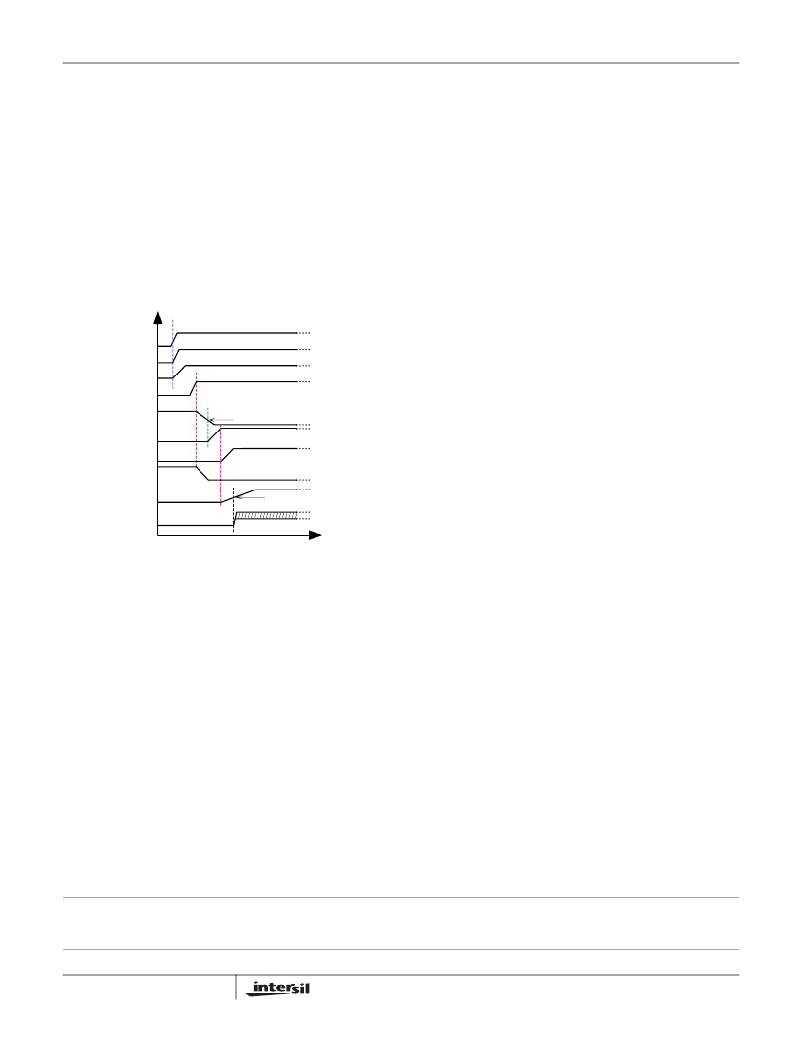
�When� EN� is� taken� high,� voltage� of� pin� PROT� and� V� OFF� start�
�ramping� down.� Once� the� PROT� voltage� falls� below� 0.9V,�
�A� VDD� starts� up� with� a� 9ms� fixed� soft-start� time.� Please� note� if�
�V� OFF� is� to� start� earlier� than� A� VDD� ,� then� the� SUPN� needs� to�
�connect� to� V� IN� ,� and� V� IN� voltage� should� be� larger� than� V� OFF�
�absolute� value.� The� delay� between� V� OFF� and� A� VDD� can� be�
���t� DELAY� =� (� V� IN� –� 0.9V� )� ×� C� 30� ?� (� 50� μ� A� )� (EQ.� 23)�
�The� successful� completion� of� the� A� VDD� soft-start� cycle�
�triggers� two� simultaneous� events.� V� ON� begins� to� ramp� up�
�and� the� voltage� on� CDEL� starts� ramping� up.� When� the�
�voltage� reaches� 1.215V,� V� ON� slice� starts.�
�V� IN�
�VREF�
�V� LOGIC�
�EN�
�Fault� Sequencing�
�The� ISL97653A� has� advanced� overall� fault� detection�
�systems� including� Overcurrent� Protection� (OCP)� for� both�
�boost� and� buck� converters,� Undervoltage� Lockout� Protection�
�(UVLP)� and� Over-Temperature� Protection.�
�Once� the� peak� current� flowing� through� the� switching�
�MOSFET� of� the� boost� and� buck� converters� triggers� the�
�current� limit� threshold,� the� PWM� comparator� will� disable� the�
�output,� cycle� by� cycle,� until� the� current� is� back� to� normal.�
�Layout� Recommendation�
�The� device's� performance� including� efficiency,� output� noise,�
�transient� response� and� control� loop� stability� is� dramatically�
�affected� by� the� PCB� layout.� PCB� layout� is� critical,� especially�
�at� high� switching� frequency.�
�There� are� some� general� guidelines� for� layout:�
�1.� Place� the� external� power� components� (the� input�
�capacitors,� output� capacitors,� boost� inductor� and� output�
�diodes,� etc.)� in� close� proximity� to� the� device.� Traces� to�
�these� components� should� be� kept� as� short� and� wide� as�
�PROT�
�A� VDD�
�V� ON�
�V� OFF�
�CDEL�
�0.9V�
�2.8V�
�1.215V�
�possible� to� minimize� parasitic� inductance� and� resistance.�
�2.� Place� V� REF� and� V� L� bypass� capacitors� close� to� the� pins.�
�3.� Reduce� the� loop� with� large� AC� amplitudes� and� fast� slew�
�rate.�
�4.� The� feedback� network� should� sense� the� output� voltage�
�directly� from� the� point� of� load,� and� be� as� far� away� from� LX�
�node� as� possible.�
�V� ON� Slice�
�*� For� demonstration� only,� not� to� scale�
�FIGURE� 18.�
�Temperature� Sensor�
�The� ISL97653A� also� includes� a� temperature� output� for� use�
�in� system� thermal� management� control.� The� integrated�
�sensor� measures� the� die� temperature� over� the� -40°C� to�
�+150°C� range.� Output� is� in� the� form� of� an� analog� voltage� on�
�the� TEMP� pin� in� the� range� of� 0V� to� 3V,� which� is� proportional�
�to� the� sensed� die� temperature.� Temperature� accuracy� is�
�±8.5°C� over� the� -40°C� to� +150°C� temperature� range.�
�The� device� should� be� disabled� by� the� user� when� the� TEMP�
�pin� output� reaches� 3V� (� =� +150°C� die� junction).� Operation� of�
�the� device� between� +125°C� and� +150°C� can� be� tolerated� for�
�short� periods,� however� in� order� to� maximize� the� life� of� the� IC,�
�it� is� recommended� that� the� effective� continuous� operating�
�5.� The� power� ground� (PGND)� and� signal� ground� (SGND)�
�pins� should� be� connected� at� only� one� point.�
�6.� The� exposed� die� plate,� on� the� underneath� of� the�
�package,� should� be� soldered� to� an� equivalent� area� of�
�metal� on� the� PCB.� This� contact� area� should� have� multiple�
�via� connections� to� the� back� of� the� PCB� as� well� as�
�connections� to� intermediate� PCB� layers,� if� available,� to�
�maximize� thermal� dissipation� away� from� the� IC.�
�7.� To� minimize� the� thermal� resistance� of� the� package� when�
�soldered� to� a� multi-layer� PCB,� the� amount� of� copper� track�
�and� ground� plane� area� connected� to� the� exposed� die�
�plate� should� be� maximized� and� spread� out� as� far� as�
�possible� from� the� IC.� The� bottom� and� top� PCB� areas�
�especially� should� be� maximized� to� allow� thermal�
�dissipation� to� the� surrounding� air.�
�8.� Minimize� feedback� input� track� lengths� to� avoid� switching�
�noise� pick-up.�
�A� demo� board� is� available� to� illustrate� the� proper� layout�
�implementation.�
�junction� temperature� of� the� die� should� not� exceed� +125°C.�
�All� Intersil� U.S.� products� are� manufactured,� assembled� and� tested� utilizing� ISO9000� quality� systems.�
�Intersil� Corporation’s� quality� certifications� can� be� viewed� at� www.intersil.com/design/quality�
�Intersil� products� are� sold� by� description� only.� Intersil� Corporation� reserves� the� right� to� make� changes� in� circuit� design,� software� and/or� specifications� at� any� time� without�
�notice.� Accordingly,� the� reader� is� cautioned� to� verify� that� data� sheets� are� current� before� placing� orders.� Information� furnished� by� Intersil� is� believed� to� be� accurate� and�
�reliable.� However,� no� responsibility� is� assumed� by� Intersil� or� its� subsidiaries� for� its� use;� nor� for� any� infringements� of� patents� or� other� rights� of� third� parties� which� may� result�
�from� its� use.� No� license� is� granted� by� implication� or� otherwise� under� any� patent� or� patent� rights� of� Intersil� or� its� subsidiaries.�
�For� information� regarding� Intersil� Corporation� and� its� products,� see� www.intersil.com�
�17�
�FN6367.3�
�September� 7,� 2010�
�相关PDF资料 |
PDF描述 |
|---|---|
| ISL97656IRTZ | IC REG BOOST ADJ 4A 10TDFN |
| ISL97701IRZ | IC REG BOOST ADJ 0.1A 10DFN |
| ISL97702IRZ-T7 | IC REG BOOST ADJ 0.13A DL 10DFN |
| ISL98012IUZ | IC REG BOOST ADJ 0.6A 10MSOP |
| ISPPAC-POWR1208-01TN44E | IC ISP POWER MGR ANLG/LOG 44TQFP |
相关代理商/技术参数 |
参数描述 |
|---|---|
| ISL97653AIRZ-T | 功能描述:电流型 PWM 控制器 5-CH INTEGRTD LCD SUPPLY W/TEMP SENSOR RoHS:否 制造商:Texas Instruments 开关频率:27 KHz 上升时间: 下降时间: 工作电源电压:6 V to 15 V 工作电源电流:1.5 mA 输出端数量:1 最大工作温度:+ 105 C 安装风格:SMD/SMT 封装 / 箱体:TSSOP-14 |
| ISL97653AIRZ-TK | 功能描述:电流型 PWM 控制器 5-CH INTEGRTD LCD SUPPLY W/TEMP SENSOR RoHS:否 制造商:Texas Instruments 开关频率:27 KHz 上升时间: 下降时间: 工作电源电压:6 V to 15 V 工作电源电流:1.5 mA 输出端数量:1 最大工作温度:+ 105 C 安装风格:SMD/SMT 封装 / 箱体:TSSOP-14 |
| ISL97653IRZ | 制造商:Intersil Corporation 功能描述: |
| ISL97656IRTZ | 功能描述:IC REG BOOST ADJ 4A 10TDFN RoHS:是 类别:集成电路 (IC) >> PMIC - 稳压器 - DC DC 开关稳压器 系列:- 产品培训模块:Lead (SnPb) Finish for COTS Obsolescence Mitigation Program 标准包装:2,500 系列:- 类型:降压(降压) 输出类型:两者兼有 输出数:1 输出电压:5V,1 V ~ 10 V 输入电压:3.5 V ~ 28 V PWM 型:电流模式 频率 - 开关:220kHz ~ 1MHz 电流 - 输出:600mA 同步整流器:无 工作温度:-40°C ~ 125°C 安装类型:表面贴装 封装/外壳:16-SSOP(0.154",3.90mm 宽) 包装:带卷 (TR) 供应商设备封装:16-QSOP |
| ISL97656IRTZEVALZ | 功能描述:EVAL BOARD FOR ISL97656IRTZ RoHS:是 类别:编程器,开发系统 >> 评估板 - DC/DC 与 AC/DC(离线)SMPS 系列:* 产品培训模块:Obsolescence Mitigation Program 标准包装:1 系列:True Shutdown™ 主要目的:DC/DC,步升 输出及类型:1,非隔离 功率 - 输出:- 输出电压:- 电流 - 输出:1A 输入电压:2.5 V ~ 5.5 V 稳压器拓扑结构:升压 频率 - 开关:3MHz 板类型:完全填充 已供物品:板 已用 IC / 零件:MAX8969 |
发布紧急采购,3分钟左右您将得到回复。