- 您现在的位置:买卖IC网 > PDF目录19807 > ISPLSI 1032E-70LJNI (Lattice Semiconductor Corporation)IC PLD ISP 64I/O 15NS 84PLCC PDF资料下载
参数资料
| 型号: | ISPLSI 1032E-70LJNI |
| 厂商: | Lattice Semiconductor Corporation |
| 文件页数: | 10/17页 |
| 文件大小: | 0K |
| 描述: | IC PLD ISP 64I/O 15NS 84PLCC |
| 标准包装: | 15 |
| 系列: | ispLSI® 1000E |
| 可编程类型: | 系统内可编程 |
| 最大延迟时间 tpd(1): | 15.0ns |
| 电压电源 - 内部: | 4.5 V ~ 5.5 V |
| 逻辑元件/逻辑块数目: | 32 |
| 门数: | 6000 |
| 输入/输出数: | 64 |
| 工作温度: | -40°C ~ 85°C |
| 安装类型: | 表面贴装 |
| 封装/外壳: | 84-LCC(J 形引线) |
| 供应商设备封装: | 84-PLCC(29.31x29.31) |
| 包装: | 管件 |
| 其它名称: | 220-1594-5 ISPLSI 1032E-70LJNI-ND ISPLSI1032E-70LJNI |
2
Specifications ispLSI 1032E
USE
ispLSI
1032EA
FOR
NEW
DESIGNS
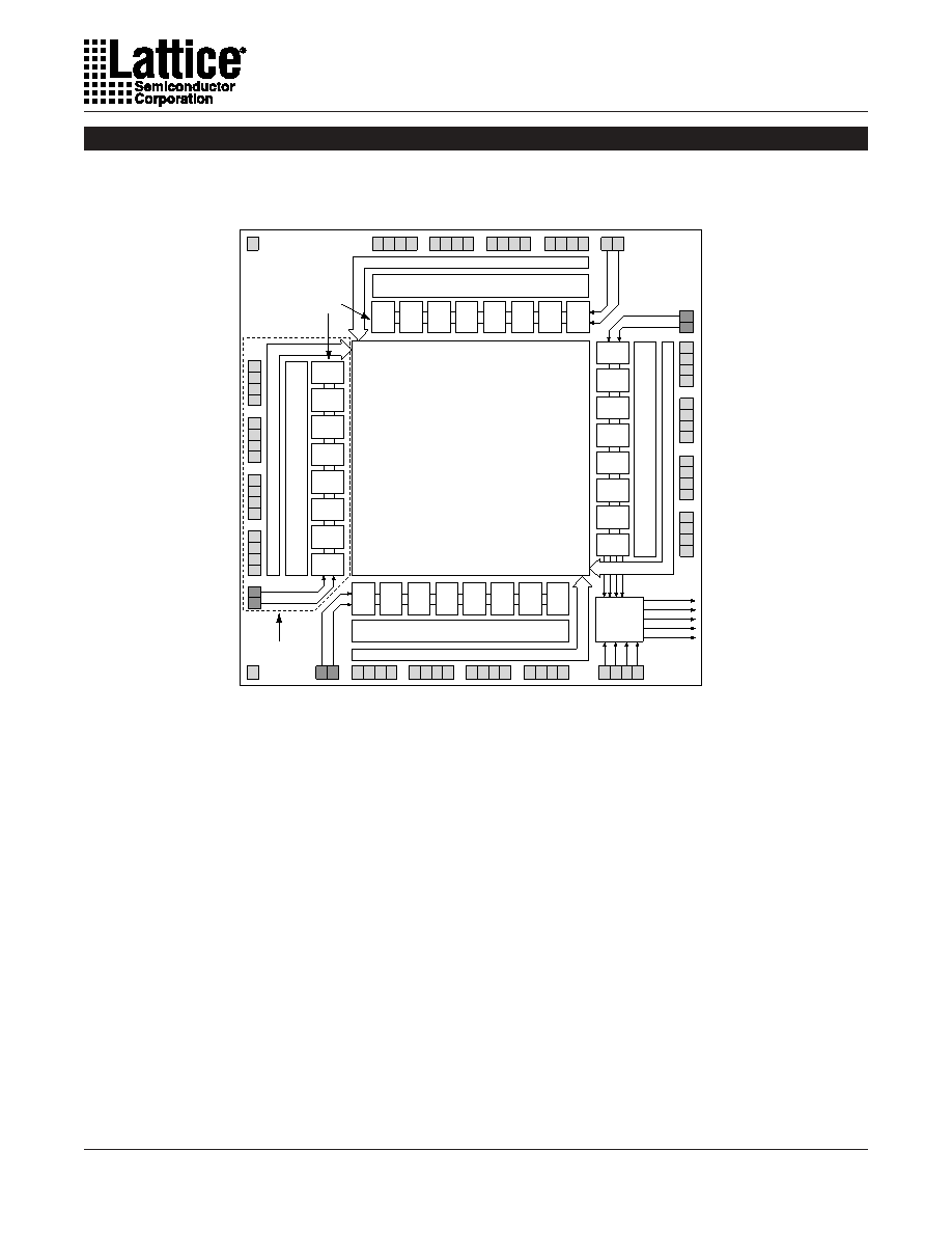
Functional Block Diagram
Figure 1. ispLSI 1032E Functional Block Diagram
The device also has 64 I/O cells, each of which is directly
connected to an I/O pin. Each I/O cell can be individually
programmed to be a combinatorial input, registered in-
put,
latched
input,
output
or
bi-directional
I/O pin with 3-state control. The signal levels are TTL
compatible voltages and the output drivers can source 4
mA or sink 8 mA. Each output can be programmed
independently for fast or slow output slew rate to mini-
mize overall output switching noise.
Eight GLBs, 16 I/O cells, two dedicated inputs and one
ORP are connected together to make a Megablock (see
Figure 1). The outputs of the eight GLBs are connected
to a set of 16 universal I/O cells by the ORP. Each ispLSI
1032E device contains four Megablocks.
The GRP has, as its inputs, the outputs from all of the
GLBs and all of the inputs from the bi-directional I/O cells.
All of these signals are made available to the inputs of the
GLBs. Delays through the GRP have been equalized to
minimize timing skew.
Clocks in the ispLSI 1032E device are selected using the
Clock Distribution Network. Four dedicated clock pins
(Y0, Y1, Y2 and Y3) are brought into the distribution
network, and five clock outputs (CLK 0, CLK 1, CLK 2,
IOCLK 0 and IOCLK 1) are provided to route clocks to the
GLBs and I/O cells. The Clock Distribution Network can
also be driven from a special clock GLB (C0 on the ispLSI
1032E device). The logic of this GLB allows the user to
create an internal clock from a combination of internal
signals within the device.
I/O
63
I/O
62
I/O
61
I/O
60
RESET
Global
Routing
Pool
(GRP)
CLK 0
CLK 1
CLK 2
IOCLK 0
IOCLK 1
Clock
Distribution
Network
C7
C6
C5
C4
C3
C2
C1
C0
A0
A1
A2
A3
A4
A5
A6
A7
Generic
Logic Blocks
(GLBs)
Megablock
Output
Routing
Pool
(ORP)
Output
Routing
Pool
(ORP)
Output Routing Pool (ORP)
Input Bus
ispEN
lnput
Bus
lnput
Bus
I/O
59
I/O
58
I/O
57
I/O
56
I/O
55
I/O
54
I/O
53
I/O
52
I/O
51
I/O
50
I/O
49
I/O
48
IN
7
IN
6
D7
D6
D5
D4
D3
D2
D1
D0
I/O
16
I/O
17
I/O
18
I/O
19
SDO/IN
2
SCLK/IN
3
I/O
20
I/O
21
I/O
22
I/O
23
I/O
24
I/O
25
I/O
26
I/O
27
I/O
28
I/O
29
I/O
30
I/O
31
I/O 35
I/O 34
I/O 33
I/O 32
I/O 0
I/O 1
I/O 2
I/O 3
I/O 12
I/O 13
I/O 14
I/O 15
SDI/IN 0
MODE/IN 1
I/O 8
I/O 9
I/O 10
I/O 11
I/O 4
I/O 5
I/O 6
I/O 7
I/O 47
I/O 46
I/O 45
I/O 44
GOE 1/IN 5
GOE 0/IN 4
I/O 43
I/O 42
I/O 41
I/O 40
I/O 39
I/O 38
I/O 37
I/O 36
Y0
Y1
Y2
Y3
B0
B1
B2
B3
B4
B5
B6
B7
相关PDF资料 |
PDF描述 |
|---|---|
| MIC29503BU | IC REG LDO ADJ 5A TO263-5 |
| VE-2WP-CY-F3 | CONVERTER MOD DC/DC 13.8V 50W |
| ISL6140IBZ | IC CONTROLLER HOT PLUG 8-SOIC |
| 10018784-11003TLF | CONN PCI EXPRESS 164POS VERT PCB |
| GSM08DRSH-S288 | CONN EDGECARD 16POS .156 EXTEND |
相关代理商/技术参数 |
参数描述 |
|---|---|
| ispLSI1032E-70LJNI | 功能描述:CPLD - 复杂可编程逻辑器件 USE ispMACH 4000V RoHS:否 制造商:Lattice 系列: 存储类型:EEPROM 大电池数量:128 最大工作频率:333 MHz 延迟时间:2.7 ns 可编程输入/输出端数量:64 工作电源电压:3.3 V 最大工作温度:+ 90 C 最小工作温度:0 C 封装 / 箱体:TQFP-100 |
| ISPLSI1032E70LT | 制造商:LATTICE 功能描述:* |
| ispLSI1032E-70LT | 功能描述:CPLD - 复杂可编程逻辑器件 USE ispMACH 4000V RoHS:否 制造商:Lattice 系列: 存储类型:EEPROM 大电池数量:128 最大工作频率:333 MHz 延迟时间:2.7 ns 可编程输入/输出端数量:64 工作电源电压:3.3 V 最大工作温度:+ 90 C 最小工作温度:0 C 封装 / 箱体:TQFP-100 |
| ISPLSI1032E70LTI | 制造商:LATTICE 制造商全称:Lattice Semiconductor 功能描述:In-System Programmable High Density PLD |
| ispLSI1032E-70LTI | 功能描述:CPLD - 复杂可编程逻辑器件 USE ispMACH 4000V RoHS:否 制造商:Lattice 系列: 存储类型:EEPROM 大电池数量:128 最大工作频率:333 MHz 延迟时间:2.7 ns 可编程输入/输出端数量:64 工作电源电压:3.3 V 最大工作温度:+ 90 C 最小工作温度:0 C 封装 / 箱体:TQFP-100 |
发布紧急采购,3分钟左右您将得到回复。