- 您现在的位置:买卖IC网 > PDF目录19807 > ISPLSI 1032E-70LJNI (Lattice Semiconductor Corporation)IC PLD ISP 64I/O 15NS 84PLCC PDF资料下载
参数资料
| 型号: | ISPLSI 1032E-70LJNI |
| 厂商: | Lattice Semiconductor Corporation |
| 文件页数: | 5/17页 |
| 文件大小: | 0K |
| 描述: | IC PLD ISP 64I/O 15NS 84PLCC |
| 标准包装: | 15 |
| 系列: | ispLSI® 1000E |
| 可编程类型: | 系统内可编程 |
| 最大延迟时间 tpd(1): | 15.0ns |
| 电压电源 - 内部: | 4.5 V ~ 5.5 V |
| 逻辑元件/逻辑块数目: | 32 |
| 门数: | 6000 |
| 输入/输出数: | 64 |
| 工作温度: | -40°C ~ 85°C |
| 安装类型: | 表面贴装 |
| 封装/外壳: | 84-LCC(J 形引线) |
| 供应商设备封装: | 84-PLCC(29.31x29.31) |
| 包装: | 管件 |
| 其它名称: | 220-1594-5 ISPLSI 1032E-70LJNI-ND ISPLSI1032E-70LJNI |
13
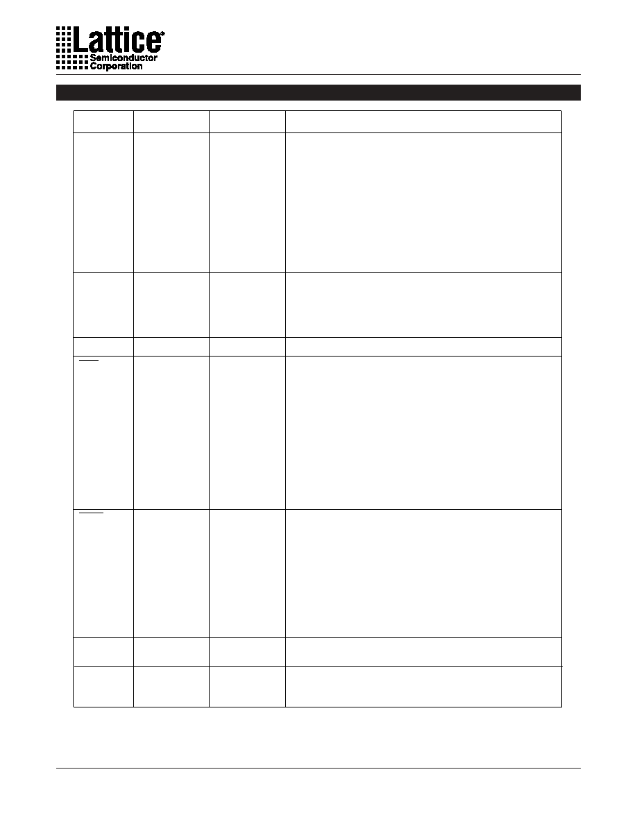
Specifications ispLSI 1032E
USE
ispLSI
1032EA
FOR
NEW
DESIGNS
Pin Description
Input - This pin performs two functions. When
ispEN is logic low, it functions
as pin to control the operation of the isp state machine. It is a dedicated
input pin when
ispEN is logic high.
This is a dual function pin. It can be used either as Global Output Enable for
all I/O cells or it can be used as a dedicated input pin.
This is a dual function pin. It can be used either as Global Output Enable for
all I/O cells or it can be used as a dedicated input pin.
Dedicated Clock input. This clock input is brought into the clock distribution
network, and can optionally be routed to any GLB on the device.
Dedicated Clock input. This clock input is connected to one of the clock
inputs of all of the GLBs on the device.
Input/Output Pins - These are the general purpose I/O pins used by the logic
array.
NAME
Table 2-0002A/1032E
PLCC PIN
NUMBERS
DESCRIPTION
26,
30,
34,
38,
45,
49,
53,
57,
68,
72,
76,
80,
3,
7,
11,
15,
27,
31,
35,
39,
46,
50,
54,
58,
69,
73,
77,
81,
4,
8,
12,
16,
28,
32,
36,
40,
47,
51,
55,
59,
70,
74,
78,
82,
5,
9,
13,
17,
I/O 0 - I/O 3
I/O 4 - I/O 7
I/O 8 - I/O 11
I/O 12 - I/O 15
I/O 16 - I/O 19
I/O 20 - I/O 23
I/O 24 - I/O 27
I/O 28 - I/O 31
I/O 32 - I/O 35
I/O 36 - I/O 39
I/O 40 - I/O 43
I/O 44 - I/O 47
I/O 48 - I/O 51
I/O 52 - I/O 55
I/O 56 - I/O 59
I/O 60 - I/O 63
29,
33,
37,
41,
48,
52,
56,
60,
71,
75,
79,
83,
6,
10,
14,
18
66
Y1
20
Y0
42
MODE/IN 12
Ground (GND)
GND
Vcc
VCC
21, 65
NC1
GOE 0/IN 43
Dedicated input pins to the device.
IN 6, IN 7
GOE 1/IN 53
2,
84
67
19
Input - Dedicated in-system programming enable input pin. This pin is
brought low to enable the programming mode. The MODE, SDI, SDO and
SCLK options become active.
23
ispEN
Input - This pin performs two functions. When
ispEN is logic low, it functions
as an input pin to load programming data into the device. SDI/IN 0 is also
used as one of the two control pins for the isp state machine. It is a
dedicated input pin when
ispEN is logic high.
25
SDI/IN 02
44
SDO/IN 22
Output/Input - This pin performs two functions. When
ispEN is logic low, it
functions as an output pin to read serial shift register data. It is a dedicated
input pin when
ispEN is logic high.
61
SCLK/IN 32
Input - This pin performs two functions. When
ispEN is logic low, it functions
as a clock pin for the Serial Shift Register. It is a dedicated input pin when
ispEN is logic high.
Active Low (0) Reset pin which resets all of the GLB and I/O registers in the
device.
24
RESET
Dedicated Clock input. This clock input is brought into the clock distribution
network, and can optionally be routed to any GLB and/or any I/O cell on the
device.
63
Y2
Dedicated Clock input. This clock input is brought into the clock distribution
network, and can optionally be routed to any I/O cell on the device.
62
Y3
1,
22,
43,
64
12,
1,
26,
51,
76,
64
2,
24, 25,
No connect.
27,
49, 50,
52,
74, 75,
77,
99, 100
1. NC pins are not to be connected to any active signals, Vcc or GND.
2. Pins have dual function capability.
3. Pins have dual function capability which is software selectable.
TQFP PIN
NUMBERS
17,
21,
29,
33,
40,
44,
48,
56,
67,
71,
79,
83,
90,
94,
98,
6,
18,
22,
30,
34,
41,
45,
53,
57,
68,
72,
80,
84,
91,
95,
3,
7,
19,
23,
31,
35,
42,
46,
54,
58,
69,
73,
81,
85,
92,
96,
4,
8,
20,
28,
32,
36,
43,
47,
55,
59,
70,
78,
82,
86,
93,
97,
5,
9
65
11
37
89,
87
66
10
14
16
39
60
15
62
61
13, 38,
63,
88
相关PDF资料 |
PDF描述 |
|---|---|
| MIC29503BU | IC REG LDO ADJ 5A TO263-5 |
| VE-2WP-CY-F3 | CONVERTER MOD DC/DC 13.8V 50W |
| ISL6140IBZ | IC CONTROLLER HOT PLUG 8-SOIC |
| 10018784-11003TLF | CONN PCI EXPRESS 164POS VERT PCB |
| GSM08DRSH-S288 | CONN EDGECARD 16POS .156 EXTEND |
相关代理商/技术参数 |
参数描述 |
|---|---|
| ispLSI1032E-70LJNI | 功能描述:CPLD - 复杂可编程逻辑器件 USE ispMACH 4000V RoHS:否 制造商:Lattice 系列: 存储类型:EEPROM 大电池数量:128 最大工作频率:333 MHz 延迟时间:2.7 ns 可编程输入/输出端数量:64 工作电源电压:3.3 V 最大工作温度:+ 90 C 最小工作温度:0 C 封装 / 箱体:TQFP-100 |
| ISPLSI1032E70LT | 制造商:LATTICE 功能描述:* |
| ispLSI1032E-70LT | 功能描述:CPLD - 复杂可编程逻辑器件 USE ispMACH 4000V RoHS:否 制造商:Lattice 系列: 存储类型:EEPROM 大电池数量:128 最大工作频率:333 MHz 延迟时间:2.7 ns 可编程输入/输出端数量:64 工作电源电压:3.3 V 最大工作温度:+ 90 C 最小工作温度:0 C 封装 / 箱体:TQFP-100 |
| ISPLSI1032E70LTI | 制造商:LATTICE 制造商全称:Lattice Semiconductor 功能描述:In-System Programmable High Density PLD |
| ispLSI1032E-70LTI | 功能描述:CPLD - 复杂可编程逻辑器件 USE ispMACH 4000V RoHS:否 制造商:Lattice 系列: 存储类型:EEPROM 大电池数量:128 最大工作频率:333 MHz 延迟时间:2.7 ns 可编程输入/输出端数量:64 工作电源电压:3.3 V 最大工作温度:+ 90 C 最小工作温度:0 C 封装 / 箱体:TQFP-100 |
发布紧急采购,3分钟左右您将得到回复。