- 您现在的位置:买卖IC网 > PDF目录22130 > ISPLSI 2032VE-110LTN48 (Lattice Semiconductor Corporation)IC PLD ISP 32I/O 10NS 48TQFP PDF资料下载
参数资料
| 型号: | ISPLSI 2032VE-110LTN48 |
| 厂商: | Lattice Semiconductor Corporation |
| 文件页数: | 10/16页 |
| 文件大小: | 0K |
| 描述: | IC PLD ISP 32I/O 10NS 48TQFP |
| 标准包装: | 250 |
| 系列: | ispLSI® 2000VE |
| 可编程类型: | 系统内可编程 |
| 最大延迟时间 tpd(1): | 10.0ns |
| 电压电源 - 内部: | 3 V ~ 3.6 V |
| 逻辑元件/逻辑块数目: | 8 |
| 宏单元数: | 32 |
| 门数: | 1000 |
| 输入/输出数: | 32 |
| 工作温度: | 0°C ~ 70°C |
| 安装类型: | 表面贴装 |
| 封装/外壳: | 48-LQFP |
| 供应商设备封装: | 48-TQFP(7x7) |
| 包装: | 托盘 |
| 其它名称: | ISPLSI2032VE-110LTN48 |
Specifications ispLSI 2032VE
2
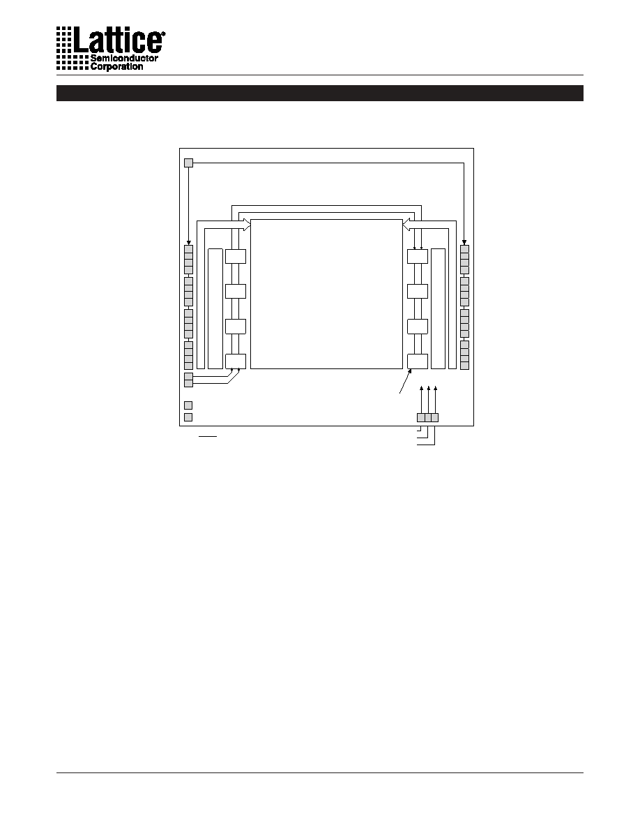
Functional Block Diagram
Figure 1. ispLSI 2032VE Functional Block Diagram
The device also has 32 I/O cells, each of which is directly
connected to an I/O pin. Each I/O cell can be individually
programmed to be a combinatorial input, output or bi-
directional I/O pin with 3-state control. The signal levels
are TTL compatible voltages and the output drivers can
source 4 mA or sink 8 mA. Each output can be pro-
grammed independently for fast or slow output slew rate
to minimize overall output switching noise. Device pins
can be safely driven to 5 Volt signal levels to support
mixed-voltage systems.
Eight GLBs, 32 I/O cells, two dedicated inputs and two
ORPs are connected together to make a Megablock (see
Figure 1). The outputs of the eight GLBs are connected
to a set of 32 universal I/O cells by the ORPs. Each
ispLSI 2032VE device contains one Megablock.
The GRP has as its inputs the outputs from all of the GLBs
and all of the inputs from the bi-directional I/O cells. All of
these signals are made available to the inputs of the
GLBs. Delays through the GRP have been equalized to
minimize timing skew.
Clocks in the ispLSI 2032VE device are selected using
the dedicated clock pins. Three dedicated clock pins (Y0,
Y1, Y2) or an asynchronous clock can be selected on a
GLB basis. The asynchronous or Product Term clock
can be generated in any GLB for its own clock.
Programmable Open-Drain Outputs
In addition to the standard output configuration, the
outputs of the ispLSI 2032VE are individually program-
mable, either as a standard totem-pole output or an
open-drain output. The totem-pole output drives the
specified Voh and Vol levels, whereas the open-drain
output drives only the specified Vol. The Voh level on the
open-drain output depends on the external loading and
pull-up. This output configuration is controlled by a pro-
grammable fuse. The default configuration when the
device is in bulk erased state is the totem-pole configu-
ration. The open-drain/totem-pole option is selectable
through the Lattice design tools.
Global Routing Pool
(GRP)
A0
A1
A3
Input
Bus
Output
Routing
Pool
(ORP)
A7
A6
A5
A4
Input
Bus
Output
Routing
Pool
(ORP)
A2
CLK
0
CLK
1
CLK
2
GOE 0
Note: *Y1 and RESET are multiplexed on the same pin
I/O 0
I/O 1
I/O 2
I/O 3
I/O 6
I/O 7
I/O 8
I/O 9
I/O 10
I/O 11
I/O 12
I/O 13
I/O 14
I/O 15
I/O 31
I/O 30
I/O 29
I/O 28
I/O 27
I/O 26
I/O 25
I/O 24
I/O 23
I/O 22
I/O 21
I/O 20
I/O 19
I/O 18
I/O 17
I/O 16
TDI/IN 0
TDO/IN 1
I/O 4
I/O 5
Y0
Y1*
TCK/Y2
BSCAN
TMS/NC
0139B/2032VE
Generic Logic
Blocks (GLBs)
SELECT
DEVICES
DISCONTINUED
相关PDF资料 |
PDF描述 |
|---|---|
| TAJC225M035SNJ | CAP TANT 2.2UF 35V 20% 2312 |
| RMM30DTBT-S189 | CONN EDGECARD 60POS R/A .156 SLD |
| LTC4240IGN | IC CTRLR HOT SWAP CPCI 28-SSOP |
| RGM30DTBT-S189 | CONN EDGECARD 60POS R/A .156 SLD |
| R2S8-2415/P | CONV DC/DC 2W 24VIN 15VOUT SMD |
相关代理商/技术参数 |
参数描述 |
|---|---|
| ispLSI2032VE-110LTN48 | 功能描述:CPLD - 复杂可编程逻辑器件 USE ispMACH 4000V RoHS:否 制造商:Lattice 系列: 存储类型:EEPROM 大电池数量:128 最大工作频率:333 MHz 延迟时间:2.7 ns 可编程输入/输出端数量:64 工作电源电压:3.3 V 最大工作温度:+ 90 C 最小工作温度:0 C 封装 / 箱体:TQFP-100 |
| ISPLSI2032VE110LTN48I | 制造商:LATTICE 制造商全称:Lattice Semiconductor 功能描述:3.3V In-System Programmable High Density SuperFAST⑩ PLD |
| ISPLSI2032VE135LB49 | 制造商:LATTICE 制造商全称:Lattice Semiconductor 功能描述:3.3V In-System Programmable High Density SuperFAST⑩ PLD |
| ISPLSI2032VE-135LB49 | 制造商:LATTICE 制造商全称:Lattice Semiconductor 功能描述:3.3V In-System Programmable High Density SuperFAST⑩ PLD |
| ISPLSI2032VE135LB49I | 制造商:LATTICE 制造商全称:Lattice Semiconductor 功能描述:3.3V In-System Programmable High Density SuperFAST⑩ PLD |
发布紧急采购,3分钟左右您将得到回复。