- 您现在的位置:买卖IC网 > PDF目录299231 > ITT3107BD RF/MICROWAVE WIDE BAND HIGH POWER AMPLIFIER PDF资料下载
参数资料
| 型号: | ITT3107BD |
| 元件分类: | 放大器 |
| 英文描述: | RF/MICROWAVE WIDE BAND HIGH POWER AMPLIFIER |
| 封装: | PLASTIC, SO-16 |
| 文件页数: | 3/4页 |
| 文件大小: | 223K |
| 代理商: | ITT3107BD |
4.8V 3.0W RF Power Amplifier IC for GSM
ITT3107BD
PRELIMINARY
Preliminary Data - Specifications Subject to Change Without Notice
901788 D, February 1999
GaAsTEK
5310 Valley Park Drive
Roanoke, VA 24019 USA
www.gaastek.com
Tel:
1-540-563-3949
1-888-563-3949 (USA)
Fax: 1-540-563-8616
3
TYPICAL CHARACTERISTICS
0
5
10
15
20
25
30
35
40
45
50
-6
-4
-2
0
2
4
6
PIN, Input Power (dBm)
P
OUT
,Output
Power
(dBm)
-2.5
-2.0
-1.5
-1.0
-0.5
0.0
V
GG
,Control
Voltage
= 897 MHz
VDD = 4.8 V
POUT
η
VGG
0
5
10
15
20
25
30
35
40
45
50
825
850
875
900
925
950
975
, Frequency (MHz)
P
OUT
(dBm),
and
η
(%)
-2.5
-2.0
-1.5
-1.0
-0.5
0.0
V
GG
,Control
Voltage
η
V
GG
P
OUT
V
DD = 4.8 V
P
IN = 0 dBm
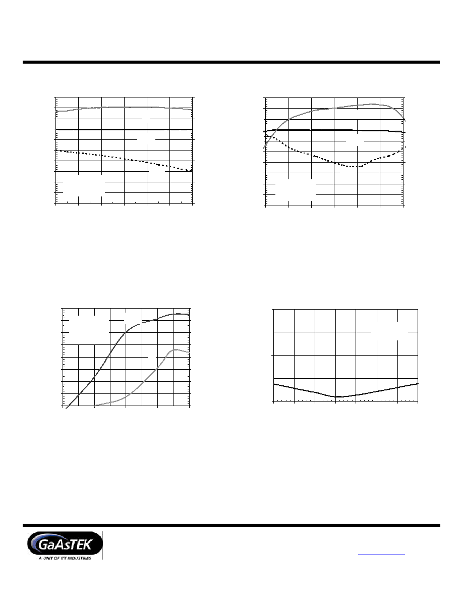
Figure 2. Output Power, Efficiency and Control
Voltage vs. Input Power
Figure 3. Output Power, Efficiency and Control Voltage
vs. Frequency
Conditions for Figure 2: Control voltage (VGG) is adjusted
at each input power level to maintain 3.0 W output power.
Conditions for Figure 3: Control voltage (VGG) is adjusted
at each frequency to maintain 3.0 W output power.
-40
-30
-20
-10
0
10
20
30
40
-2.2
-2.0
-1.8
-1.6
-1.4
VGG, Control Voltage (Volts)
P
OUT
,Output
Power
(dBm)
0
10
20
30
40
50
60
70
80
η
,Pwr
Added
Efficiency
(%)
POUT
η
= 897 MHz
VDD = 4.8 V
PIN = 0 dBm
1:1
2:1
3:1
880
885
890
895
900
905
910
915
, Frequency (MHz)
Input
VSWR
VDD = 4.8 V
PIN = 0 dBm
Figure 4. Output Power and Efficiency vs. Control
Voltage
Figure 5. Input VSWR vs. Frequency
Conditions for Figure 5: Control voltage (VGG) is adjusted
at each frequency to maintain 3.0 W output power.
相关PDF资料 |
PDF描述 |
|---|---|
| ITTS402AH | RF/MICROWAVE SGL POLE FOUR THROW SWITCH |
| IXBOD1-21R | 2100 V, RVS BLOCKING BOD |
| IXFN64N50PD2 | |
| IXFT80N08 | 80 A, 80 V, 0.009 ohm, N-CHANNEL, Si, POWER, MOSFET, TO-268 |
| IXFX26N120P | 26 A, 1200 V, 0.46 ohm, N-CHANNEL, Si, POWER, MOSFET |
相关代理商/技术参数 |
参数描述 |
|---|---|
| ITT333105BD | 制造商:Micronas 功能描述: |
| ITT35V1000UF | 制造商:IFF 功能描述:RL810X035 TYPE CEUS 16X26 105C |
| ITT4-AH | 制造商:FUJITSU Component Ltd 功能描述: 制造商:FUJITSU 功能描述: |
| ITT4-AR | 制造商:FUJITSU Component Ltd 功能描述: 制造商:FUJITSU 功能描述: |
| ITT4B-AR | 制造商:FUJITSU Component Ltd 功能描述: |
发布紧急采购,3分钟左右您将得到回复。