- 您现在的位置:买卖IC网 > Datasheet目录335 > IXDD404SIA-16 (IXYS)IC MOSFET DRVR DUAL 4A 16-SOIC Datasheet资料下载
参数资料
| 型号: | IXDD404SIA-16 |
| 厂商: | IXYS |
| 文件页数: | 11/12页 |
| 文件大小: | 0K |
| 描述: | IC MOSFET DRVR DUAL 4A 16-SOIC |
| 产品变化通告: | Discontinuation Notice 15/Jun/2010 |
| 标准包装: | 46 |
| 配置: | 低端 |
| 输入类型: | 非反相 |
| 延迟时间: | 36ns |
| 电流 - 峰: | 4A |
| 配置数: | 2 |
| 输出数: | 2 |
| 电源电压: | 4.5 V ~ 35 V |
| 工作温度: | -55°C ~ 125°C |
| 安装类型: | 表面贴装 |
| 封装/外壳: | 16-SOIC(0.295",7.50mm 宽) |
| 供应商设备封装: | 16-SOIC |
| 包装: | 管件 |
| 配用: | EVDD404-ND - EVALUATION BOARD FOR IXDD404 DVR |
�� �
�
�IXDD404�
�Supply Bypassing and Grounding Practices,�
�Output Lead inductance�
�When� designing� a� circuit� to� drive� a� high� speed� MOSFET�
�utilizing� the� IXDD404,� it� is� very� important� to� keep� certain� design�
�criteria� in� mind,� in� order� to� optimize� performance� of� the� driver.�
�Particular� attention� needs� to� be� paid� to� Supply� Bypassing� ,�
�Grounding� ,� and� minimizing� the� Output� Lead� Inductance� .�
�Say,� for� example,� we� are� using� the� IXDD404� to� charge� a� 2500pF�
�capacitive� load� from� 0� to� 25� volts� in� 25ns� .�
�Using� the� formula:� I=� ?� V� C� /� ?� t,� where� ?� V=25V� C=2500pF� &�
�?� t=25ns� we� can� determine� that� to� charge� 2500pF� to� 25� volts� in�
�25ns� will� take� a� constant� current� of� 2.5A.� (In� reality,� the� charging�
�current� won’t� be� constant,� and� will� peak� somewhere� around�
�4A).�
�SUPPLY� BYPASSING�
�In� order� for� our� design� to� turn� the� load� on� properly,� the� IXDD404�
�must� be� able� to� draw� this� 2.5A� of� current� from� the� power� supply�
�in� the� 25ns.� This� means� that� there� must� be� very� low� impedance�
�between� the� driver� and� the� power� supply.� The� most� common�
�method� of� achieving� this� low� impedance� is� to� bypass� the� power�
�supply� at� the� driver� with� a� capacitance� value� that� is� a� magnitude�
�larger� than� the� load� capacitance.� Usually,� this� would� be�
�achieved� by� placing� two� different� types� of� bypassing� capacitors,�
�with� complementary� impedance� curves,� very� close� to� the� driver�
�itself.� (These� capacitors� should� be� carefully� selected,� low�
�inductance,� low� resistance,� high-pulse� current-service�
�capacitors).� Lead� lengths� may� radiate� at� high� frequency� due�
�to� inductance,� so� care� should� be� taken� to� keep� the� lengths� of�
�the� leads� between� these� bypass� capacitors� and� the� IXDD404�
�to� an� absolute� minimum.�
�GROUNDING�
�In� order� for� the� design� to� turn� the� load� off� properly,� the� IXDD404�
�must� be� able� to� drain� this� 2.5A� of� current� into� an� adequate�
�grounding� system.� There� are� three� paths� for� returning� current�
�that� need� to� be� considered:� Path� #1� is� between� the� IXDD404�
�and� it’s� load.� Path� #2� is� between� the� IXDD404� and� it’s� power�
�supply.� Path� #3� is� between� the� IXDD404� and� whatever� logic�
�is� driving� it.� All� three� of� these� paths� should� be� as� low� in�
�resistance� and� inductance� as� possible,� and� thus� as� short� as�
�practical.� In� addition,� every� effort� should� be� made� to� keep� these�
�three� ground� paths� distinctly� separate.� Otherwise,� (for�
�instance),� the� returning� ground� current� from� the� load� may�
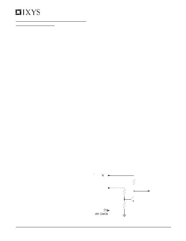
�TTL to High Voltage CMOS Level Translation�
�The� enable� (EN)� input� to� the� IXDD404� is� a� high� voltage�
�CMOS� logic� level� input� where� the� EN� input� threshold� is� ?�
�V� CC� ,� and� may� not� be� compatible� with� 5V� CMOS� or� TTL� input�
�levels.� The� IXDD404� EN� input� was� intentionally� designed�
�for� enhanced� noise� immunity� with� the� high� voltage� CMOS�
�logic� levels.� In� a� typical� gate� driver� application,� V� CC� =15V�
�and� the� EN� input� threshold� at� 7.5V,� a� 5V� CMOS� logical� high�
�input� applied� to� this� typical� IXDD404� application’s� EN� input�
�will� be� misinterpreted� as� a� logical� low,� and� may� cause�
�undesirable� or� unexpected� results.� The� note� below� is� for�
�optional� adaptation� of� TTL� or� 5V� CMOS� levels.�
�The� circuit� in� Figure� 28� alleviates� this� potential� logic� level�
�misinterpretation� by� translating� a� TTL� or� 5V� CMOS� logic�
�input� to� high� voltage� CMOS� logic� levels� needed� by� the�
�IXDD404� EN� input.� From� the� figure,� V� CC� is� the� gate� driver�
�power� supply,� typically� set� between� 8V� to� 20V,� and� V� DD� is� the�
�logic� power� supply,� typically� between� 3.3V� to� 5.5V.�
�Resistors� R1� and� R2� form� a� voltage� divider� network� so� that�
�the� Q1� base� is� positioned� at� the� midpoint� of� the� expected�
�TTL� logic� transition� levels.�
�A� TTL� or� 5V� CMOS� logic� low,� V� TTLLOW� =~<0.8V,� input� applied�
�to� the� Q1� emitter� will� drive� it� on.� This� causes� the� level�
�translator� output,� the� Q1� collector� output� to� settle� to� V� CESATQ1�
�+� V� TTLLOW� =<~2V,� which� is� sufficiently� low� to� be� correctly�
�interpreted� as� a� high� voltage� CMOS� logic� low� (<1/3V� CC� =5V�
�for� V� CC� =15V� given� in� the� IXDD404� data� sheet.)�
�A� TTL� high,� V� TTLHIGH� =>~2.4V,� or� a� 5V� CMOS� high,�
�V� 5VCMOSHIGH� =~>3.5V,� applied� to� the� EN� input� of� the� circuit� in�
�Figure� 28� will� cause� Q1� to� be� biased� off.� This� results� in� Q1�
�collector� being� pulled� up� by� R3� to� V� CC� =15V,� and� provides� a�
�high� voltage� CMOS� logic� high� output.� The� high� voltage�
�CMOS� logical� EN� output� applied� to� the� IXDD404� EN� input�
�will� enable� it,� allowing� the� gate� driver� to� fully� function� as� a�
�±� 4� Amp� output� driver.�
�The� total� component� cost� of� the� circuit� in� Figure� 28� is� less�
�than� $0.10� if� purchased� in� quantities� >1K� pieces.� It� is�
�recommended� that� the� physical� placement� of� the� level�
�translator� circuit� be� placed� close� to� the� source� of� the� TTL� or�
�CMOS� logic� circuits� to� maximize� noise� rejection.�
�Figure� 30� -� TTL� to� High� Voltage� CMOS� Level� Translator�
�develop� a� voltage� that� would� have� a� detrimental� effect� on� the�
�logic� line� driving� the� IXDD404.�
�OUTPUT� LEAD� INDUCTANCE�
�CC�
�(From� Gate� Driver�
�Power� Supply)�
�10K�
�R3�
�Of� equal� importance� to� Supply� Bypassing� and� Grounding� are�
�issues� related� to� the� Output� Lead� Inductance.� Every� effort�
�should� be� made� to� keep� the� leads� between� the� driver� and� it’s�
�load� as� short� and� wide� as� possible.� If� the� driver� must� be� placed�
�farther� than� 2”� from� the� load,� then� the� output� leads� should� be�
�V� DD�
�(From� Logic�
�Power� Supply)�
�3.3K�
�R1�
�Q1�
�2N3904�
�High� Voltage�
�CMOS� EN�
�Output�
�(To� IXDD404�
�EN� Input)�
�treated� as� transmission� lines.� In� this� case,� a� twisted-pair�
�should� be� considered,� and� the� return� line� of� each� twisted� pair�
�should� be� placed� as� close� as� possible� to� the� ground� pin� of� the�
�driver,� and� connect� directly� to� the� ground� terminal� of� the�
�load.�
�11�
�or� TTL� Input)�
�3.3K�
�R2�
�相关PDF资料 |
PDF描述 |
|---|---|
| IXDD408YI | IC MOSFET DRVR LS 8A SGL 5TO-263 |
| IXDD414SI | IC MOSFET DRVR 14A LOSIDE 14SOIC |
| IXDD509D1T/R | IC GATE DRIVER 9A 6-DFN |
| IXDD614CI | MOSFET N-CH 14A LO SIDE TO-220-5 |
| IXDE504SIAT/R | IC GATE DRIVER 4A 8-SOIC |
相关代理商/技术参数 |
参数描述 |
|---|---|
| IXDD408CI | 功能描述:功率驱动器IC 40V 8A RoHS:否 制造商:Micrel 产品:MOSFET Gate Drivers 类型:Low Cost High or Low Side MOSFET Driver 上升时间: 下降时间: 电源电压-最大:30 V 电源电压-最小:2.75 V 电源电流: 最大功率耗散: 最大工作温度:+ 85 C 安装风格:SMD/SMT 封装 / 箱体:SOIC-8 封装:Tube |
| IXDD408PI | 功能描述:功率驱动器IC 40V 8A RoHS:否 制造商:Micrel 产品:MOSFET Gate Drivers 类型:Low Cost High or Low Side MOSFET Driver 上升时间: 下降时间: 电源电压-最大:30 V 电源电压-最小:2.75 V 电源电流: 最大功率耗散: 最大工作温度:+ 85 C 安装风格:SMD/SMT 封装 / 箱体:SOIC-8 封装:Tube |
| IXDD408SI | 功能描述:功率驱动器IC 40V 8A RoHS:否 制造商:Micrel 产品:MOSFET Gate Drivers 类型:Low Cost High or Low Side MOSFET Driver 上升时间: 下降时间: 电源电压-最大:30 V 电源电压-最小:2.75 V 电源电流: 最大功率耗散: 最大工作温度:+ 85 C 安装风格:SMD/SMT 封装 / 箱体:SOIC-8 封装:Tube |
| IXDD408YI | 功能描述:功率驱动器IC 40V 8A RoHS:否 制造商:Micrel 产品:MOSFET Gate Drivers 类型:Low Cost High or Low Side MOSFET Driver 上升时间: 下降时间: 电源电压-最大:30 V 电源电压-最小:2.75 V 电源电流: 最大功率耗散: 最大工作温度:+ 85 C 安装风格:SMD/SMT 封装 / 箱体:SOIC-8 封装:Tube |
| IXDD409CI | 功能描述:功率驱动器IC 9 Amps 40V 1.5 Rds RoHS:否 制造商:Micrel 产品:MOSFET Gate Drivers 类型:Low Cost High or Low Side MOSFET Driver 上升时间: 下降时间: 电源电压-最大:30 V 电源电压-最小:2.75 V 电源电流: 最大功率耗散: 最大工作温度:+ 85 C 安装风格:SMD/SMT 封装 / 箱体:SOIC-8 封装:Tube |
发布紧急采购,3分钟左右您将得到回复。